Part 1
요약·해설
16개 지원 interface, LED·button·UART pin, 외부 J-Link와 USB-TTL 절차, 10 kHz pin 제약을 설명합니다.
nRF52840 · Cortex-M4F
1 MB flash · 256 KB RAM
QSPI · USB
Part 2
접을 수 있는 영어 원문 전체
영어 원문 전체 펼치기
9833F8F4C697DFF9B0E674E7F50DC3F45B15D3E26A49142876F542B2AB089402
.. _raytac_mdbt50q_db_40_nrf52840:

Raytac MDBT50Q-DB-40
####################

Overview
********

The Raytac MDBT50Q-DB-40 hardware provides support for the
Nordic Semiconductor nRF52840 ARM Cortex-M4F CPU and the following devices:

* :abbr:`ADC (Analog to Digital Converter)`
* CLOCK
* FLASH
* :abbr:`GPIO (General Purpose Input Output)`
* :abbr:`I2C (Inter-Integrated Circuit)`
* :abbr:`MPU (Memory Protection Unit)`
* :abbr:`NVIC (Nested Vectored Interrupt Controller)`
* :abbr:`PWM (Pulse Width Modulation)`
* RADIO (Bluetooth Low Energy and 802.15.4)
* :abbr:`RTC (nRF RTC System Clock)`
* Segger RTT (RTT Console)
* :abbr:`SPI (Serial Peripheral Interface)`
* :abbr:`UART (Universal asynchronous receiver-transmitter)`
* :abbr:`USB (Universal Serial Bus)`
* :abbr:`WDT (Watchdog Timer)`

.. figure:: ../../../../../../../boards/raytac/mdbt50q_db_40/doc/img/mdbt50q_db_40.jpg
     :width: 442px
     :align: center
     :alt: MDBT50Q-DB-40

More information about the board can be found at the `MDBT50Q-DB-40 website`_.
The `MDBT50Q-DB-40 Specification`_ contains the demo board's datasheet.
The `MDBT50Q-DB-40 Schematic`_ contains the demo board's schematic.

Hardware
********
- Module Demo Board build by MDBT50Q-1MV2
- Nordic nRF52840 SoC Solution Version: 2
- A recommnded 3rd-party module by Nordic Semiconductor.
- BT5.2&BT5.1&BT5 Bluetooth Specification Cerified
- Supports BT5 Long Range Features
- Cerifications: FCC, IC, CE, Telec(MIC), KC, SRRC, NCC, RCM, WPC
- 32-bit ARM® Cortex™ M4F CPU
- 1MB Flash Memory/256kB RAM
- RoHs & Reach Compiant.
- 48 GPIO
- Chip Antenna
- Interfaces: SPI, UART, I2C, I2S, PWM, ADC, NFC, and USB
- Highly flexible multiprotocol SoC ideally suited for Bluetooth® Low Energy, ANT+, Zigbee, Thread (802.15.4) ultra low-power wireless applications.
- 3 User LEDs
- 4 User buttons
- 1 Mini USB connector for power supply and USB communication
- SWD connector for FW programing
- J-Link interface for FW programing
- UART interface for UART communication

Supported Features
==================

The raytac_mdbt50q_db_40/nrf52840 board configuration supports the following
hardware features:

+-----------+------------+----------------------+
| Interface | Controller | Driver/Component     |
+===========+============+======================+
| ADC       | on-chip    | adc                  |
+-----------+------------+----------------------+
| CLOCK     | on-chip    | clock_control        |
+-----------+------------+----------------------+
| FLASH     | on-chip    | flash                |
+-----------+------------+----------------------+
| GPIO      | on-chip    | gpio                 |
+-----------+------------+----------------------+
| I2C(M)    | on-chip    | i2c                  |
+-----------+------------+----------------------+
| MPU       | on-chip    | arch/arm             |
+-----------+------------+----------------------+
| NVIC      | on-chip    | arch/arm             |
+-----------+------------+----------------------+
| PWM       | on-chip    | pwm                  |
+-----------+------------+----------------------+
| RADIO     | on-chip    | Bluetooth,           |
|           |            | ieee802154           |
+-----------+------------+----------------------+
| RTC       | on-chip    | system clock         |
+-----------+------------+----------------------+
| RTT       | Segger     | console              |
+-----------+------------+----------------------+
| SPI(M/S)  | on-chip    | spi                  |
+-----------+------------+----------------------+
| QSPI(M)   | on-chip    | qspi                 |
+-----------+------------+----------------------+
| UART      | on-chip    | serial               |
+-----------+------------+----------------------+
| USB       | on-chip    | usb                  |
+-----------+------------+----------------------+
| WDT       | on-chip    | watchdog             |
+-----------+------------+----------------------+

Other hardware features have not been enabled yet for this board.
See `MDBT50Q-DB-40 website`_ and `MDBT50Q-DB-40 Specification`_
for a complete list of Raytac MDBT50Q-DB-40 board hardware features.

Connections and IOs
===================

LED
---

* LED1 (green) = P0.13
* LED2 (red) = P0.14
* LED3 (blue) = P0.15

Push buttons
------------

* BUTTON1 = SW1 = P0.11
* BUTTON2 = SW2 = P0.12
* BUTTON3 = SW3 = P0.24
* BUTTON4 = SW4 = P0.25

UART
----
* RXD = P0.08
* TXD = P0.06
* RTS = P0.05
* CTS = P0.07

Programming and Debugging
*************************

Applications for the ``raytac_mdbt50q_db_40/nrf52840`` board configuration can be
built, flashed, and debugged in the usual way. See :ref:`build_an_application` and
:ref:`application_run` for more details on building and running.

.. note::
   Flashing and Debugging Zephyr onto the raytac_mdbt50q_db_40/nrf52840 board
   requires an	external J-Link programmer. The programmer is attached to the J1
   or J9 SWD connector.

Flashing
========

Follow the instructions in the :ref:`nordic_segger` page to install
and configure all the necessary software. Further information can be
found in :ref:`nordic_segger_flashing`. Then build and flash
applications as usual (see :ref:`build_an_application` and
:ref:`application_run` for more details).

Here is an example for the :ref:`hello_world` application.

Use a USB to TTL converter to connect the computer and raytac_mdbt50q_db_40/nrf52840
J10 connector. Then run your favorite terminal program to listen for output.

.. code-block:: console

   $ minicom -D <tty_device> -b 115200

Replace :code:`<tty_device>` with the port where the USB to TTL converter
can be found. For example, under Linux, :code:`/dev/ttyUSB0`.

Then build and flash the application in the usual way.

.. zephyr-app-commands::
   :zephyr-app: samples/hello_world
   :board: raytac_mdbt50q_db_40/nrf52840
   :goals: build flash

Debugging
=========

The ``raytac_mdbt50q_db_40/nrf52840`` board does not have an on-board-J-Link debug IC,
however, instructions from the :ref:`nordic_segger` page also apply to this board.
Use the Debug out connector of nRF52x DK to connect to the J1 connector, and use SEGGER
J-Link OB IF to debug.

Testing the LEDs and buttons in the MDBT50Q-DB-40
*************************************************

There are 2 samples that allow you to test that the buttons (switches) and LEDs on
the board are working properly with Zephyr:

.. code-block:: console

   samples/basic/blinky
   samples/basic/button

You can build and flash the examples to make sure Zephyr is running correctly on
your board. The button and LED definitions can be found in
:zephyr_file:`boards/raytac/mdbt50q_db_40/raytac_mdbt50q_db_40_nrf52840.dts`.

Selecting the pins
==================

Pins can be configured in the board pinctrl file. To see the available mappings,
open the `MDBT50Q-DB-40 Specification`_, chapter 2.5 'Pin Assignment'.
Select the pins marked 'General-purpose I/O'. Note that pins marked as 'low-frequency I/O
only' can only be used in under-10KHz applications. They are not suitable for SPI, I2C,
UART, and PWM.

References
**********

.. target-notes::

.. _MDBT50Q-DB-40 website:
	https://www.raytac.com/product/ins.php?index_id=81
.. _MDBT50Q-DB-40 Specification:
	https://www.raytac.com/download/index.php?index_id=43
.. _MDBT50Q-DB-40 Schematic:
	https://www.raytac.com/upload/catalog_b/134ade06b5db3dd5803d27c5b17f22f3.jpg
.. _J-Link Software and documentation pack:
	https://www.segger.com/jlink-software.html
Part 3
한국어 전문 번역
개요
Raytac MDBT50Q-DB-40 hardware는 Nordic Semiconductor nRF52840 ARM Cortex-M4F CPU와 다음 장치를 지원합니다.
- ADC (Analog-to-Digital Converter)
- CLOCK
- FLASH
- GPIO (General Purpose Input/Output)
- I2C (Inter-Integrated Circuit)
- MPU (Memory Protection Unit)
- NVIC (Nested Vectored Interrupt Controller)
- PWM (Pulse Width Modulation)
- RADIO (Bluetooth Low Energy 및 802.15.4)
- RTC (nRF RTC system clock)
- SEGGER RTT (RTT console)
- SPI (Serial Peripheral Interface)
- UART (Universal asynchronous receiver-transmitter)
- USB (Universal Serial Bus)
- WDT (Watchdog Timer)
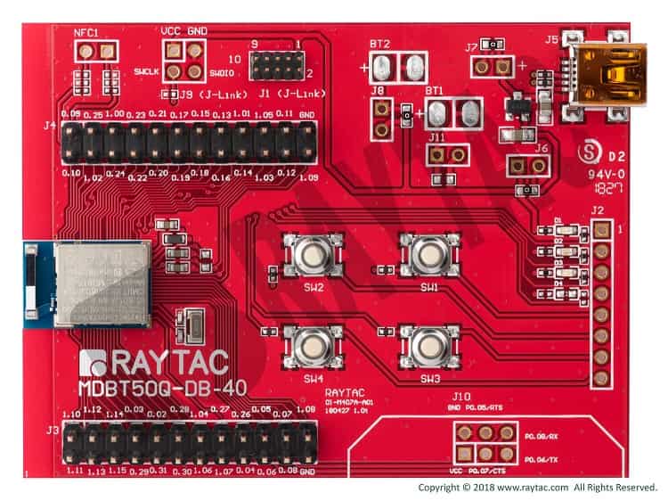
보드의 자세한 정보는 MDBT50Q-DB-40 website에서 확인할 수 있습니다. MDBT50Q-DB-40 specification에는 demo board datasheet가, MDBT50Q-DB-40 schematic에는 회로도가 있습니다.

하드웨어
- MDBT50Q-1MV2으로 만든 module demo board
- Nordic nRF52840 SoC solution version 2
- Nordic Semiconductor가 권장하는 third-party module
- Bluetooth 5.2, 5.1, 5 specification 인증
- Bluetooth 5 Long Range feature 지원
- FCC, IC, CE, Telec(MIC), KC, SRRC, NCC, RCM, WPC 인증
- 32-bit ARM® Cortex™-M4F CPU
- 1 MB flash memory / 256 KB RAM
- RoHS 및 REACH 준수
- 48 GPIO
- Chip antenna
- SPI, UART, I2C, I2S, PWM, ADC, NFC, USB interface
- Bluetooth® Low Energy, ANT+, Zigbee, Thread(802.15.4) 초저전력 wireless application에 적합한 유연한 multiprotocol SoC
- User LED 3개
- User button 4개
- 전원 공급 및 USB 통신용 Mini USB connector 1개
- Firmware programming용 SWD connector
- Firmware programming용 J-Link interface
- UART 통신용 UART interface
지원 기능
raytac_mdbt50q_db_40/nrf52840 board configuration은 다음 hardware feature를 지원합니다.
| 인터페이스 | 컨트롤러 | 드라이버/컴포넌트 |
|---|---|---|
ADC | on-chip | adc |
CLOCK | on-chip | clock_control |
FLASH | on-chip | flash |
GPIO | on-chip | gpio |
I2C(M) | on-chip | i2c |
MPU | on-chip | arch/arm |
NVIC | on-chip | arch/arm |
PWM | on-chip | pwm |
RADIO | on-chip | Bluetooth, ieee802154 |
RTC | on-chip | system clock |
RTT | Segger | console |
SPI(M/S) | on-chip | spi |
QSPI(M) | on-chip | qspi |
UART | on-chip | serial |
USB | on-chip | usb |
WDT | on-chip | watchdog |
그 밖의 hardware feature는 아직 이 보드에서 활성화되지 않았습니다. 전체 목록은 MDBT50Q-DB-40 website와 MDBT50Q-DB-40 specification을 참고합니다.
연결과 I/O
LED
- LED1(green) = P0.13
- LED2(red) = P0.14
- LED3(blue) = P0.15
Push button
- BUTTON1 = SW1 = P0.11
- BUTTON2 = SW2 = P0.12
- BUTTON3 = SW3 = P0.24
- BUTTON4 = SW4 = P0.25
UART
- RXD = P0.08
- TXD = P0.06
- RTS = P0.05
- CTS = P0.07
프로그래밍과 디버깅
raytac_mdbt50q_db_40/nrf52840용 application은 일반적인 방법으로 build, flash, debug할 수 있습니다. 자세한 build와 실행 방법은 Zephyr의 application build/run 문서를 따릅니다.
플래시
Zephyr Nordic SEGGER 문서에 따라 필요한 software를 설치하고 구성한 뒤 평소와 같이 application을 build하고 flash합니다. 다음은 hello_world 예입니다.
USB-to-TTL converter로 computer와 raytac_mdbt50q_db_40/nrf52840의 J10 connector를 연결하고 terminal program으로 출력을 수신합니다.
$ minicom -D <tty_device> -b 115200<tty_device>를 USB-to-TTL converter가 나타나는 port로 바꿉니다. Linux에서는 예를 들어 /dev/ttyUSB0입니다. 그런 다음 application을 build하고 flash합니다.
west build -b raytac_mdbt50q_db_40/nrf52840 samples/hello_world
west flash
디버깅
raytac_mdbt50q_db_40/nrf52840 board에는 on-board J-Link debug IC가 없지만 Zephyr Nordic SEGGER 지침을 그대로 적용할 수 있습니다. nRF52x DK의 Debug out connector를 J1 connector에 연결하고 SEGGER J-Link OB interface로 debug합니다.
MDBT50Q-DB-40 LED와 button 시험
다음 두 sample로 보드의 button(switch)과 LED가 Zephyr에서 올바르게 동작하는지 시험할 수 있습니다.
samples/basic/blinky
samples/basic/button
Example을 build하고 flash해 Zephyr가 보드에서 제대로 실행되는지 확인할 수 있습니다. Button과 LED definition은 boards/raytac/mdbt50q_db_40/raytac_mdbt50q_db_40_nrf52840.dts에 있습니다.
Pin 선택
Pin은 board pinctrl file에서 구성할 수 있습니다. 가능한 mapping은 MDBT50Q-DB-40 specification의 2.5절 “Pin Assignment”를 엽니다. “General-purpose I/O”로 표시된 pin을 선택합니다. “low-frequency I/O only”로 표시된 pin은 10 kHz 미만 application에서만 사용할 수 있으며 SPI, I2C, UART, PWM에는 적합하지 않습니다.
참고 자료
Source
출처
영어 원문에는 문단, 문서 지시문, 표, 코드, 코드 심벌, 경로를 그대로 보존했습니다.