Part 1
요약·해설
지원 기능 4종, connector·GPIO 59행, SPI/I2C/UART/CAN alternate function과 flash/debug 명령을 보존했습니다.
STM32F405RG · Cortex-M4
UEXT · 35-pin function rows
ST-Link V2 · external JTAG
Part 2
접을 수 있는 영어 원문 전체
영어 원문 전체 펼치기
828B27EEDF0D6AB5BDCD8B2DC7E4B236AB32FD8CA9939EBEC70A3A56CAD9111D
.. _olimex_stm32_p405:

OLIMEX-STM32-P405
#################

Overview
********

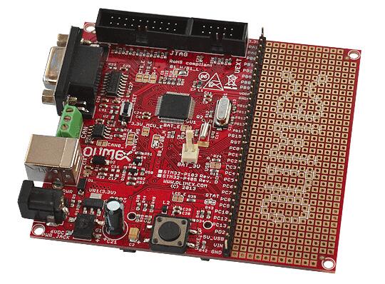
The OLIMEX-STM32-P405 board is based on the STMicroelectronics STM32F405RG ARM
Cortex-M4 CPU.

.. figure:: ../../../../../../../boards/olimex/stm32_p405/doc/img/olimex_stm32_p405.jpg
     :align: center
     :alt: OLIMEX-STM32-P405

     OLIMEX-STM32-P405

Hardware
********

Information about the board can be found at the
`OLIMEX-STM32-P405 website`_ and `OLIMEX-STM32-P405 user manual`_.
The `ST STM32F405RG Datasheet`_ contains the processor's
information and the datasheet.

Supported Features
==================

The olimex_stm32_p405 board configuration supports the following
hardware features:

+-----------+------------+----------------------+
| Interface | Controller | Driver/Component     |
+===========+============+======================+
| NVIC      | on-chip    | nested vectored      |
|           |            | interrupt controller |
+-----------+------------+----------------------+
| SYSTICK   | on-chip    | system clock         |
+-----------+------------+----------------------+
| UART      | on-chip    | serial port          |
+-----------+------------+----------------------+
| GPIO      | on-chip    | gpio                 |
+-----------+------------+----------------------+

Other hardware features have not been enabled yet for this board.

Pin Mapping
===========

.. figure:: ../../../../../../../boards/olimex/stm32_p405/doc/img/olimex-stm32-p405-front.jpg
     :align: center
     :alt: OLIMEX-STM32-P405 connectors

     OLIMEX-STM32-P405 connectors

LED
---

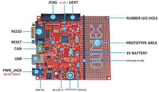
* USER_LED (red) = PC12
* PWR_LED (red) = power

Push buttons
------------

* USER_BUTTON = PA0
* RST = NRST

External Connectors
-------------------

JTAG debug

+-------+--------------+-------+--------------+
| PIN # | Signal Name  | Pin # | Signal Name  |
+=======+==============+=======+==============+
| 1     | +3.3V        | 11    | -            |
+-------+--------------+-------+--------------+
| 2     | +3.3V        | 12    | GND          |
+-------+--------------+-------+--------------+
| 3     | PB4 / TRST   | 13    | PB3 / TDO    |
+-------+--------------+-------+--------------+
| 4     | GND          | 14    | GND          |
+-------+--------------+-------+--------------+
| 5     | PA15 / TDI   | 15    | PB4 / TRST   |
+-------+--------------+-------+--------------+
| 6     | GND          | 16    | GND          |
+-------+--------------+-------+--------------+
| 7     | PA13 / TMS   | 17    | -            |
+-------+--------------+-------+--------------+
| 8     | GND          | 18    | GND          |
+-------+--------------+-------+--------------+
| 9     | PA14 / TCK   | 19    | +5V_JTAG     |
+-------+--------------+-------+--------------+
| 10    | GND          | 20    | GND          |
+-------+--------------+-------+--------------+

UEXT

+-------+-----------------------+----------------+
| PIN # | Wire   Name           | STM32F405 port |
+=======+=======================+================+
| 1     | +3.3V                 | -              |
+-------+-----------------------+----------------+
| 2     | GND                   | -              |
+-------+-----------------------+----------------+
| 3     | PA9/USART1_TX         | PA9            |
+-------+-----------------------+----------------+
| 4     | PA10/USART1_RX        | PA10           |
+-------+-----------------------+----------------+
| 5     | PB6/I2C1_SCL          | PB6            |
+-------+-----------------------+----------------+
| 6     | PB7/I2C1_SDA          | PB7            |
+-------+-----------------------+----------------+
| 7     | PA6/SPI1_MISO         | PA6            |
+-------+-----------------------+----------------+
| 8     | PA7/SPI1_MOSI         | PA7            |
+-------+-----------------------+----------------+
| 9     | PA5/SPI1_SCK          | PA5            |
+-------+-----------------------+----------------+
| 10    | PA4/SPI1_NSS          | PA4            |
+-------+-----------------------+----------------+


GPIO row of pins

+---------+----------------------------------------------+
| Pin     | STM32F405 Pin Functions                      |
+=========+==============================================+
| 3V3     | N/A                                          |
+---------+----------------------------------------------+
| PA1     | PA1/USART2_RTS/ADC1/TIM2_CH2                 |
+---------+----------------------------------------------+
| PA8     | PA8/USART1_CK/TIM1_CH1/MCO                   |
+---------+----------------------------------------------+
| PB0     | PB0/ADC8/TIM3_CH3/TIM1_CH2N                  |
+---------+----------------------------------------------+
| PB1     | PB1/ADC9/TIM3_CH4/TIM1_CH3N                  |
+---------+----------------------------------------------+
| PB2     | PB2/BOOT1                                    |
+---------+----------------------------------------------+
| PB5     | PB5/I2C1_SMBAI/TIM3_CH2/SPI1_MOSI            |
+---------+----------------------------------------------+
| PB8     | PB8/TIM4_CH3/I2C1_SCL/CANRX                  |
+---------+----------------------------------------------+
| PB9     | PB9/TIM4_CH4/I2C1_SDA/CANTX                  |
+---------+----------------------------------------------+
| VDDA    | N/A                                          |
+---------+----------------------------------------------+
| GNDA    | N/A                                          |
+---------+----------------------------------------------+
| PB10    | PB10/I2C2_SCL/USART3_TX/TIM2_CH3             |
+---------+----------------------------------------------+
| PB11    | PB11/I2C2_SDA/USART3_RX/TIM2_CH4             |
+---------+----------------------------------------------+
| PB12    | PB12/SPI2_NSS/I2C2_SMBAL/USART3_CK/TIM1_BKIN |
+---------+----------------------------------------------+
| PB13    | PB13/SPI2_SCK/USART3_CTS/TIM1_CH1N           |
+---------+----------------------------------------------+
| PB14    | PB14/SPI2_MISO/USART3_RTS/TIM1_CH2N          |
+---------+----------------------------------------------+
| PB15    | PB15/SPI2_MOSI/TIM1_CH3N                     |
+---------+----------------------------------------------+
| RST     | NRST                                         |
+---------+----------------------------------------------+
| PC0     | PC0/ADC10                                    |
+---------+----------------------------------------------+
| PC1     | PC1/ADC11                                    |
+---------+----------------------------------------------+
| PC2     | PC2/ADC12                                    |
+---------+----------------------------------------------+
| PC3     | PC3/ADC13                                    |
+---------+----------------------------------------------+
| PC4     | PC4/ADC14                                    |
+---------+----------------------------------------------+
| PC5     | PC5/ADC15                                    |
+---------+----------------------------------------------+
| PC6     | PC6/TIM3_CH1                                 |
+---------+----------------------------------------------+
| PC7     | PC7/TIM3_CH2                                 |
+---------+----------------------------------------------+
| PC8     | PC8/TIM3_CH3                                 |
+---------+----------------------------------------------+
| PC9     | PC9/TIM3_CH4                                 |
+---------+----------------------------------------------+
| PC10    | PC10/USART3_TX                               |
+---------+----------------------------------------------+
| PC12    | PC12/USART3_CK                               |
+---------+----------------------------------------------+
| PC13    | PC13/ANTI_TAMP                               |
+---------+----------------------------------------------+
| PD2     | PD2/TIM3_ETR                                 |
+---------+----------------------------------------------+
| +5V_USB | N/A                                          |
+---------+----------------------------------------------+
| VIN     | N/A                                          |
+---------+----------------------------------------------+
| GND     | N/A                                          |
+---------+----------------------------------------------+


System Clock
============

OLIMEX-STM32-P405 has two external oscillators. The frequency of
the slow clock is 32.768 kHz. The frequency of the main clock
is 8 MHz. The processor can setup HSE to drive the master clock,
which can be set as high as 168 MHz.

Programming and Debugging
*************************
The OLIMEX-STM32-P405 board does not include an embedded debug tool
interface. You will need to use ST tools or an external JTAG probe.
In the following examples a ST-Link V2 USB dongle is used.

Flashing an application to the Olimex-STM32-P405
================================================

The sample application :ref:`hello_world` is being used in this tutorial.

Connect the ST-Link USB dongle to your host computer and to the JTAG port of
the OLIMEX-STM32-P405 board.

Now build and flash the application.

.. zephyr-app-commands::
   :zephyr-app: samples/hello_world
   :board: olimex_stm32_p405
   :goals: build flash

Run a serial host program to connect with your board:

.. code-block:: console

   $ minicom -D /dev/ttyACM0

After resetting the board, you should see the following message:

.. code-block:: console

   ***** BOOTING ZEPHYR OS v1.8.99 - BUILD: Aug  4 2017 14:54:40 *****
   Hello World! arm

Debugging
=========

You can debug an application in the usual way.  Here is an example for the
:ref:`hello_world` application.

.. zephyr-app-commands::
   :zephyr-app: samples/hello_world
   :board: olimex_stm32_p405
   :maybe-skip-config:
   :goals: debug

.. _OLIMEX-STM32-P405 website:
   https://www.olimex.com/Products/ARM/ST/STM32-P405/

.. _OLIMEX-STM32-P405 user manual:
   https://www.olimex.com/Products/ARM/ST/STM32-P405/resources/STM32-P405_UM.pdf

.. _ST STM32F405RG Datasheet:
   https://www.st.com/resource/en/reference_manual/dm00031020.pdf
Part 3
한국어 전문 번역
개요
OLIMEX-STM32-P405는 STMicroelectronics STM32F405RG ARM Cortex-M4 CPU 기반 보드입니다.
보드 정보는 website와 user manual, processor 정보는 ST STM32F405RG datasheet에 있습니다.
지원 기능
| 인터페이스 | 컨트롤러 | 드라이버/컴포넌트 |
|---|---|---|
NVIC | on-chip | nested vectored interrupt controller |
SYSTICK | on-chip | system clock |
UART | on-chip | serial port |
GPIO | on-chip | gpio |
표에 없는 하드웨어 기능은 아직 활성화되지 않았습니다.
핀 배치
LED와 button
- USER_LED (red):
PC12 - PWR_LED (red): power
- USER_BUTTON:
PA0 - RST:
NRST
JTAG debug
| PIN # | Signal Name | Pin # | Signal Name |
|---|---|---|---|
1 | +3.3V | 11 | - |
2 | +3.3V | 12 | GND |
3 | PB4 / TRST | 13 | PB3 / TDO |
4 | GND | 14 | GND |
5 | PA15 / TDI | 15 | PB4 / TRST |
6 | GND | 16 | GND |
7 | PA13 / TMS | 17 | - |
8 | GND | 18 | GND |
9 | PA14 / TCK | 19 | +5V_JTAG |
10 | GND | 20 | GND |
UEXT
| PIN # | Wire Name | STM32F405 port |
|---|---|---|
1 | +3.3V | - |
2 | GND | - |
3 | PA9/USART1_TX | PA9 |
4 | PA10/USART1_RX | PA10 |
5 | PB6/I2C1_SCL | PB6 |
6 | PB7/I2C1_SDA | PB7 |
7 | PA6/SPI1_MISO | PA6 |
8 | PA7/SPI1_MOSI | PA7 |
9 | PA5/SPI1_SCK | PA5 |
10 | PA4/SPI1_NSS | PA4 |
GPIO pin row
| Pin | STM32F405 Pin Functions |
|---|---|
3V3 | N/A |
PA1 | PA1/USART2_RTS/ADC1/TIM2_CH2 |
PA8 | PA8/USART1_CK/TIM1_CH1/MCO |
PB0 | PB0/ADC8/TIM3_CH3/TIM1_CH2N |
PB1 | PB1/ADC9/TIM3_CH4/TIM1_CH3N |
PB2 | PB2/BOOT1 |
PB5 | PB5/I2C1_SMBAI/TIM3_CH2/SPI1_MOSI |
PB8 | PB8/TIM4_CH3/I2C1_SCL/CANRX |
PB9 | PB9/TIM4_CH4/I2C1_SDA/CANTX |
VDDA | N/A |
GNDA | N/A |
PB10 | PB10/I2C2_SCL/USART3_TX/TIM2_CH3 |
PB11 | PB11/I2C2_SDA/USART3_RX/TIM2_CH4 |
PB12 | PB12/SPI2_NSS/I2C2_SMBAL/USART3_CK/TIM1_BKIN |
PB13 | PB13/SPI2_SCK/USART3_CTS/TIM1_CH1N |
PB14 | PB14/SPI2_MISO/USART3_RTS/TIM1_CH2N |
PB15 | PB15/SPI2_MOSI/TIM1_CH3N |
RST | NRST |
PC0 | PC0/ADC10 |
PC1 | PC1/ADC11 |
PC2 | PC2/ADC12 |
PC3 | PC3/ADC13 |
PC4 | PC4/ADC14 |
PC5 | PC5/ADC15 |
PC6 | PC6/TIM3_CH1 |
PC7 | PC7/TIM3_CH2 |
PC8 | PC8/TIM3_CH3 |
PC9 | PC9/TIM3_CH4 |
PC10 | PC10/USART3_TX |
PC12 | PC12/USART3_CK |
PC13 | PC13/ANTI_TAMP |
PD2 | PD2/TIM3_ETR |
+5V_USB | N/A |
VIN | N/A |
GND | N/A |
System clock
외부 oscillator는 slow clock 32.768 kHz와 main clock 8 MHz 두 개입니다. Processor는 HSE를 master clock source로 설정해 최대 168 MHz로 동작할 수 있습니다.
프로그래밍과 디버깅
Embedded debug interface가 없어 ST 도구나 외부 JTAG probe가 필요합니다. 아래 예는 ST-Link V2 USB dongle과 hello_world를 사용합니다.
Application flash
ST-Link를 host와 board JTAG port에 연결한 뒤 build하고 flash합니다.
# Zephyr 저장소 루트에서
west build -b olimex_stm32_p405 samples/hello_world
west flash
Serial host program으로 연결합니다.
$ minicom -D /dev/ttyACM0Reset 후 다음 메시지가 표시됩니다.
***** BOOTING ZEPHYR OS v1.8.99 - BUILD: Aug  4 2017 14:54:40 *****
Hello World! arm
Debug
# Zephyr 저장소 루트에서
west build -b olimex_stm32_p405 samples/hello_world
west debug
참고 자료
Source
출처
영어 원문에는 문단, 문서 지시문, 표, 코드, 코드 심벌, 경로를 그대로 보존했습니다.