Part 1
요약·해설
AN521은 dual Cortex-M33 SoC입니다. CPU0은 Secure·Non-Secure firmware를, CPU1은 별도 firmware를 지원하며 code/SRAM 영역을 공유하므로 target별 partition을 정확히 지켜야 합니다.
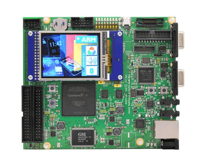
Dual Arm Cortex-M33
CPU0 S · CPU0 NS · CPU1
Armv8-M TrustZone, IDAU, MPC, PPC
Part 2
접을 수 있는 영어 원문 전체
영어 원문 전체 펼치기
FEF60C5A79672B158C4AE1709B384803AEE892C7BAEFD5CA49A6DE0A3A2C68ED
.. _mps2_an521_board:

ARM MPS2+ AN521
###############

Overview
********

The mps2/an521 board configuration is used by Zephyr applications that run
on the MPS2+ AN521 board. It provides support for the MPS2+ AN521 ARM Cortex-M33
CPU and the following devices:

- Nested Vectored Interrupt Controller (NVIC)
- System Tick System Clock (SYSTICK)
- Cortex-M System Design Kit GPIO
- Cortex-M System Design Kit UART

.. image:: ../../../../../../../boards/arm/mps2/doc/img/mps2_an521.jpg
     :align: center
     :alt: ARM MPS2+ AN521

In addition to enabling actual hardware usage, this board configuration can
also use QEMU to emulate the AN521 platform running on the MPS2+.

More information about the board can be found at the `MPS2 FPGA Website`_.

.. note::
   This board configuration makes no claims about its suitability for use
   with actual MPS2 hardware systems using AN521, or any other hardware
   system. It has been tested on actual hardware, but its primary purpose is
   for use with QEMU and unit tests for the ARM Cortex-M33.


Zephyr board options
====================

The MPS2+ AN521 is a dual core SoC with Cortex-M33 architecture on both cores
(CPU0 and CPU1). Zephyr provides support for building firmware
images for both CPU0 and CPU1. For CPU0 supporting ARM Security Extensions
both Secure and Non-Secure firmware images may be built.

The BOARD options are summarized below:

+----------------------+-------------------------------------------------------+
| BOARD                | Description                                           |
+======================+=======================================================+
| mps2/an521/cpu0      | For building Secure (or Secure-only) firmware on CPU0 |
+----------------------+-------------------------------------------------------+
| mps2/an521/cpu0/ns   | For building Non-Secure firmware for CPU0             |
+----------------------+-------------------------------------------------------+
| mps2/an521/cpu1      | For building firmware on CPU1                         |
+----------------------+-------------------------------------------------------+

Memory Partitioning
===================

The AN521 has 4MB allocated for code space, and 4MB for SRAM. These memory
regions are shared across both cores, and are aliased in both secure and
non-secure regions, where the secure memory alias has an offset of
0x10000000 relative to non-secure.

The following memory map and partitioning schemes are used by default, where
the offset value is the offset from the base of the 4MB code or SRAM block,
ignoring the S/NS alias difference.

+-------------------------+-----+----------------+----------------+------------+
| Board                   | CPU | Code (Offset)  | SRAM (Offset)  | S/NS Alias |
+=========================+=====+================+================+============+
| mps2/an521/cpu0         | 0   | 4MB (0)        | 4MB (0)        | S          |
+-------------------------+-----+----------------+----------------+------------+
| mps2/an521/cpu0/ns      | 0   | 512KB (1MB)    | 512KB (1MB)    | NS         |
+-------------------------+-----+----------------+----------------+------------+
| mps2/an521/cpu1         | 1   | 468KB (3628KB) | 512KB (1.5MB)  | NS         |
+-------------------------+-----+----------------+----------------+------------+

The ``mps2/an521/cpu0/ns`` board target is intended to be used with TF-M, with the
Zephyr memory map matching the AN521 memory map defined upstream in TF-M. TF-M
boots the secure processing environment before initialising Zephyr in the
non-secure processing environment. The non-secure Zephyr image is offset to
make room for the secure bootloader, and the secure firmware (TF-M), resulting
in a starting address of 0x00100000. SRAM begins with a 1MB offset at
0x28100000.

The ``mps2/an521/cpu1`` board target is setup for the second core on the
AN521, using the final 468KB code memory in the 4MB code block. This value
is chosen to maintain compatibility with TF-M, which marks that final 468KB
code region as ``Unused``. Code memory thus starts with an offset of
3628KB (address 0x0038B000), and sram starts with an offset of 1.5MB
(address 0x28180000).

This memory map enables the two alternative board targets to be used together
if required, at the cost of reducing the amount of code memory available on
the second core to the worst-case scenario from TF-M.

When using one of the alternative board targets (``mps2/an521/cpu0/ns`` or
``mps2/an521/cpu1``), care needs to be taken with the amount of code or
SRAM memory used on the primary board target (``mps2/an521``) since there is
some overlap in the memory maps.

Hardware
********

ARM MPS2+ AN521 provides the following hardware components:

- Dual core ARM Cortex-M33
- Soft Macro Model (SMM) implementation of SSE-200 subsystem
- Memory

  - 4MB of code memory (SSRAM1)
  - 4MB of SRAM (SSRAM2 and SSRAM3)
  - 16MB of parallel SRAM (PSRAM, non-secure only)
  - 8KB of NVM code

- Debug

  - P-JTAG, SWD & 16-bit TRACE
  - UART port

- Interface

  - AHB GPIO connected to the EXP port
  - UART
  - SPI
  - I2C
  - I2S
  - Color LCD serial interface
  - Ethernet
  - VGA

- On-board Peripherals

  - Color LCD
  - 8 LEDs
  - 8 Switches
  - External SSRAM1, SSRAM2 & SSRAM3
  - SMSC9220
  - CS42L52


User push buttons
=================

The mps2/an521 board provides the following user push buttons:

- ON power on
- nSRST: Cortex-M33 system reset and CoreSight debug reset
- USERPB0 and USERPB1: User defined buttons


Supported Features
===================

The mps2/an521 board configuration supports the following hardware features:

+-----------+------------+-------------------------------------+
| Interface | Controller | Driver/Component                    |
+===========+============+=====================================+
| NVIC      | on-chip    | nested vector interrupt controller  |
+-----------+------------+-------------------------------------+
| SYSTICK   | on-chip    | systick                             |
+-----------+------------+-------------------------------------+
| UART      | on-chip    | serial port-polling;                |
|           |            | serial port-interrupt               |
+-----------+------------+-------------------------------------+
| PINMUX    | on-chip    | pinmux                              |
+-----------+------------+-------------------------------------+
| GPIO      | on-chip    | gpio                                |
+-----------+------------+-------------------------------------+
| WATCHDOG  | on-chip    | watchdog                            |
+-----------+------------+-------------------------------------+
| TIMER     | on-chip    | timer                               |
+-----------+------------+-------------------------------------+

Other hardware features are not currently supported by the port.
See the `MPS2 FPGA Website`_ for a complete list of MPS2+ AN521 board hardware
features.

The default configuration can be found in
:zephyr_file:`boards/arm/mps2/mps2_an521_cpu0_defconfig`.

Interrupt Controller
====================

MPS2+ AN521 is a Cortex-M33 based SoC and has 15 fixed exceptions and 77 IRQs.

A Cortex-M33-based board uses vectored exceptions. This means each exception
calls a handler directly from the vector table.

Zephyr provides handlers for exceptions 1-7, 11, 12, 14, and 15, as listed
in the following table:

+------+------------+----------------+--------------------------+
| Exc# | Name       | Remarks        | Used by Zephyr Kernel    |
+======+============+================+==========================+
|  1   | Reset      |                | system initialization    |
+------+------------+----------------+--------------------------+
|  2   | NMI        |                | system fatal error       |
+------+------------+----------------+--------------------------+
|  3   | Hard fault |                | system fatal error       |
+------+------------+----------------+--------------------------+
|  4   | MemManage  | MPU fault      | system fatal error       |
+------+------------+----------------+--------------------------+
|  5   | Bus        |                | system fatal error       |
+------+------------+----------------+--------------------------+
|  6   | Usage      | Undefined      | system fatal error       |
|      | fault      | instruction,   |                          |
|      |            | or switch      |                          |
|      |            | attempt to ARM |                          |
|      |            | mode           |                          |
+------+------------+----------------+--------------------------+
|  7   | SecureFault| Unauthorized   | system fatal error       |
|      |            | access to      |                          |
|      |            | secure region  |                          |
|      |            | from ns space  |                          |
+------+------------+----------------+--------------------------+
|  8   | Reserved   |                | not handled              |
+------+------------+----------------+--------------------------+
|  9   | Reserved   |                | not handled              |
+------+------------+----------------+--------------------------+
| 10   | Reserved   |                | not handled              |
+------+------------+----------------+--------------------------+
| 11   | SVC        |                | system calls, kernel     |
|      |            |                | run-time exceptions,     |
|      |            |                | and IRQ offloading       |
+------+------------+----------------+--------------------------+
| 12   | Debug      |                | system fatal error       |
|      | monitor    |                |                          |
+------+------------+----------------+--------------------------+
| 13   | Reserved   |                | not handled              |
+------+------------+----------------+--------------------------+
| 14   | PendSV     |                | context switch           |
+------+------------+----------------+--------------------------+
| 15   | SYSTICK    |                | system clock             |
+------+------------+----------------+--------------------------+
| 16   | Reserved   |                | not handled              |
+------+------------+----------------+--------------------------+
| 17   | Reserved   |                | not handled              |
+------+------------+----------------+--------------------------+
| 18   | Reserved   |                | not handled              |
+------+------------+----------------+--------------------------+

Pin Mapping
===========

The ARM MPS2+ AN521 Board has 4 CMSDK AHB GPIO controllers. Each providing 16
bits of IO. These controllers are responsible for pin-muxing, input/output,
pull-up, etc.

All GPIO controller pins are exposed via the following sequence of pin numbers:

- Pins 0 - 15 are for GPIO0
- Pins 16 -  31 are for GPIO1
- Pins 32 -  47 are for GPIO2
- Pins 48 -  51 are for GPIO3

Mapping from the ARM MPS2+ AN521 Board pins to GPIO controllers:

.. rst-class:: rst-columns

   - D0 : EXT_0
   - D1 : EXT_4
   - D2 : EXT_2
   - D3 : EXT_3
   - D4 : EXT_1
   - D5 : EXT_6
   - D6 : EXT_7
   - D7 : EXT_8
   - D8 : EXT_9
   - D9 : EXT_10
   - D10 : EXT_12
   - D11 : EXT_13
   - D12 : EXT_14
   - D13 : EXT_11
   - D14 : EXT_15
   - D15 : EXT_5
   - D16 : EXT_16
   - D17 : EXT_17
   - D18 : EXT_18
   - D19 : EXT_19
   - D20 : EXT_20
   - D21 : EXT_21
   - D22 : EXT_22
   - D23 : EXT_23
   - D24 : EXT_24
   - D25 : EXT_25
   - D26 : EXT_26
   - D27 : EXT_30
   - D28 : EXT_28
   - D29 : EXT_29
   - D30 : EXT_27
   - D31 : EXT_32
   - D32 : EXT_33
   - D33 : EXT_34
   - D34 : EXT_35
   - D35 : EXT_36
   - D36 : EXT_38
   - D37 : EXT_39
   - D38 : EXT_40
   - D39 : EXT_44
   - D40 : EXT_41
   - D41 : EXT_31
   - D42 : EXT_37
   - D43 : EXT_42
   - D44 : EXT_43
   - D45 : EXT_45
   - D46 : EXT_46
   - D47 : EXT_47
   - D48 : EXT_48
   - D49 : EXT_49
   - D50 : EXT_50
   - D51 : EXT_51

Peripheral Mapping:

.. rst-class:: rst-columns

   - UART_3_RX : D0
   - UART_3_TX : D1
   - SPI_3_CS : D10
   - SPI_3_MOSI : D11
   - SPI_3_MISO : D12
   - SPI_3_SCLK : D13
   - I2C_3_SDA : D14
   - I2C_3_SCL : D15
   - UART_4_RX : D26
   - UART_4_TX : D30
   - SPI_4_CS : D36
   - SPI_4_MOSI : D37
   - SPI_4_MISO : D38
   - SPI_4_SCK : D39
   - I2C_4_SDA : D40
   - I2C_4_SCL : D41

For more details refer to `MPS2+ AN521 Technical Reference Manual (TRM)`_.

LED
============

MPS2+ has 8 built-in LEDs connected to Serial Configuration Controller (SCC).

.. note:: The SCC register CFG_REG1 Bits [7:0] for LEDa, 0 = OFF 1 = ON.

System Clock
============

MPS2+ AN521 has several clocks connected:

.. rst-class:: rst-columns

   - MAINCLK : 20MHz
   - SYSCLK : 20MHz
   - S32KCLK : 32kHz
   - TRACECLK : 20MHz
   - SWCLKTCK : 20MHz
   - TRACECLKIN : 20MHz

Serial Port
===========

The MPS2+ AN521 has five UARTs. The Zephyr console output by default, uses
UART0, which is J10 on the board.

UART2 is reserved. And UART 1, 3 and 4 are alt-functions on the EXP ports.

Security components
===================

- Implementation Defined Attribution Unit (`IDAU`_). The IDAU is used to define
  secure and non-secure memory maps. By default, all of the memory space is
  defined to be secure accessible only
- Secure and Non-secure peripherals via the Peripheral Protection Controller
  (PPC). Peripherals can be assigned as secure or non-secure accessible
- Secure boot
- Secure `AMBA®`_ interconnect

Serial Configuration Controller (SCC)
=====================================

The MPS2+ AN521 implements a Serial Configuration Control (SCC) register.
The purpose of this register is to allow individual control of clocks,
reset-signals and interrupts to peripherals, and pin-muxing, and the LEDs and
switches.

Programming and Debugging
*************************

MPS2+ AN521 (CPU0) supports the Armv8m Security Extension.
Applications built for the mps2/an521 board by default
boot in the Secure state.

MPS2+ AN521 (CPU1) does not support the Armv8m Security Extension.

Building Secure/Non-Secure Zephyr applications with Arm |reg| TrustZone |reg|
=============================================================================

Applications on the MPS2+ AN521 (CPU0) may contain a Secure and a Non-Secure
firmware image. The Secure image can be built using either Zephyr
or `Trusted Firmware M`_ (TF-M). Non-Secure firmware images are always built
using Zephyr. The two alternatives are described below.

.. note::

   By default the Secure image for the MPS2+ AN521 (CPU0) is built
   using TF-M.

Building the Secure firmware with TF-M
--------------------------------------

The process to build the Secure firmware image using TF-M and the Non-Secure
firmware image using Zephyr requires the following steps:

1. Build the Non-Secure Zephyr application
   for MPS2+ AN521 (CPU0) using ``-DBOARD=mps2/an521/cpu0/ns``.
   To invoke the building of TF-M the Zephyr build system requires the
   Kconfig option ``BUILD_WITH_TFM`` to be enabled, which is done by
   default when building Zephyr as a Non-Secure application.
   The Zephyr build system will perform the following steps automatically:

      * Build the Non-Secure firmware image as a regular Zephyr application
      * Build a TF-M (secure) firmware image
      * Merge the output image binaries together
      * Optionally build a bootloader image (MCUboot)

.. note::

   Depending on the TF-M configuration, an application DTS overlay may be
   required, to adjust the Non-Secure image Flash and SRAM starting address
   and sizes.

Building the Secure firmware using Zephyr
-----------------------------------------

The process to build the Secure and the Non-Secure firmware images
using Zephyr requires the following steps:

1. Build the Secure Zephyr application for MPS2+ AN521 (CPU0)
   using ``-DBOARD=mps2/an521`` and
   ``CONFIG_TRUSTED_EXECUTION_SECURE=y`` and ``CONFIG_BUILD_WITH_TFM=n``
   in the application project configuration file.
2. Build the Non-Secure Zephyr application for MPS2+ AN521 (CPU0)
   using ``-DBOARD=mps2/an521/cpu0/ns``.
3. Merge the two binaries together.

Building a Secure only application on MPS2+ AN521 (CPU0)
========================================================

Build the Zephyr app in the usual way (see :ref:`build_an_application`
and :ref:`application_run`), using ``-DBOARD=mps2/an521`` for
the firmware running on the MPS2+ AN521 (CPU0).

When building a Secure/Non-Secure application for the MPS2+ AN521 (CPU0),
the Secure application will have to set the SAU/IDAU configuration to allow
Non-Secure access to all CPU resources utilized by the Non-Secure application
firmware. SAU/IDAU configuration shall take place before jumping to the
Non-Secure application.

The following system components are required to be properly configured during the
secure firmware:

- AHB5 TrustZone Memory Protection Controller (MPC)
- AHB5 TrustZone Peripheral Protection Controller (PPC)
- Implementation-Defined Attribution Unit (IDAU)

For more details refer to `Corelink SSE-200 Subsystem`_.


Building standalone applications on MPS2+ AN521 CPU1
====================================================

Applications may be built for the second Cortex-M33
(remote) core of MPS2+ AN521. The core is referred to as CPU1.

Build the Zephyr app in the usual way (see :ref:`build_an_application`
and :ref:`application_run`), using ``-DBOARD=mps2/an521/cpu1`` for
the firmware running on the MPS2+ AN521 (CPU1).

The Zephyr build will automatically trigger building a minimal (empty)
secure-only firmware for CPU0, which will be used to boot the remote
core (CPU1).


Flashing
========

MPS2+ AN521 provides:

- A USB connection to the host computer, which exposes a Mass Storage
- A Serial Port which is J10 on MPS2+ board

Build applications as described above.
Here is an example for the :ref:`hello_world` application built as
a secure-only application for CPU0.

.. zephyr-app-commands::
   :zephyr-app: samples/hello_world
   :board: mps2/an521
   :goals: build


Open a serial terminal (minicom, putty, etc.) with the following settings:

- Speed: 115200
- Data: 8 bits
- Parity: None
- Stop bits: 1

Reset the board, and you should see the following message on the corresponding
serial port:

.. code-block:: console

   Hello World! mps2_an521


Uploading an application to MPS2+ AN521
---------------------------------------

Applications can be in elf, hex or bin format. The binaries are flashed when
the board boots up, using files stored on the on-board Micro SD card. The
Motherboard Configuration Controller (MCC) is responsible for loading the FPGA
image and binaries.

Connect the MPS2+ to your host computer using the USB port. You should see a
USB connection exposing a Mass Storage (``V2M_MPS2`` by default).

The update requires 3 steps:

1. Copy application files to ``<MPS2 device name>/SOFTWARE/``.
2. Open ``<MPS2 device name>/MB/HBI0263C/AN521/images.txt``.
3. Update the ``AN521/images.txt`` file as follows:

.. code-block:: bash

   TITLE: Versatile Express Images Configuration File

   [IMAGES]
   TOTALIMAGES: 1 ;Number of Images (Max: 32)

   IMAGE0ADDRESS: 0x10000000 ;Please select the required executable program

   IMAGE0FILE: \SOFTWARE\zephyr.bin


Reset the board, and you should see the following message on the corresponding
serial port:

.. code-block:: console

   Hello World! mps2_an521

.. note:: Refer to the tfm_integration sample for more details about integrating with TF-M and multiple images scenario.


.. _MPS2 FPGA Website:
   https://developer.arm.com/tools-and-software/development-boards/fpga-prototyping-boards/mps2

.. _MPS2+ AN521 Technical Reference Manual (TRM):
   https://developer.arm.com/documentation/dai0521/latest/

.. _Cortex M33 Generic User Guide:
   https://developer.arm.com/documentation/100235/latest/

.. _Trusted Firmware M:
   https://tf-m-user-guide.trustedfirmware.org/building/tfm_build_instruction.html

.. _Corelink SSE-200 Subsystem:
   https://developer.arm.com/documentation/dto0051/latest/subsystem-overview/about-the-sse-200

.. _IDAU:
   https://developer.arm.com/documentation/100690/latest/Attribution-units--SAU-and-IDAU-

.. _AMBA®:
   https://developer.arm.com/products/architecture/system-architectures/amba
Part 3
한국어 전문 번역
개요
mps2/an521 보드 구성은 MPS2+ AN521의 dual Arm Cortex-M33 CPU와 NVIC, SYSTICK, CMSDK GPIO·UART를 지원합니다.
실제 hardware 외에 QEMU로 MPS2+ AN521 platform을 emulation할 수 있습니다.
Zephyr board option
CPU0과 CPU1 모두 Cortex-M33입니다. CPU0은 Arm Security Extension을 지원해 Secure 및 Non-Secure image를 만들 수 있습니다.
| BOARD | 설명 |
|---|---|
mps2/an521/cpu0 | CPU0 Secure 또는 Secure-only firmware |
mps2/an521/cpu0/ns | CPU0 Non-Secure firmware |
mps2/an521/cpu1 | CPU1 firmware |
Memory partitioning
code 4 MB와 SRAM 4 MB를 두 core가 공유합니다. secure와 non-secure region에 각각 alias되며 secure alias는 non-secure보다 0x10000000 offset에 있습니다. 다음 offset은 S/NS alias 차이를 제외한 각 4 MB block base 기준입니다.
| Board | CPU | Code offset | SRAM offset | S/NS alias |
|---|---|---|---|---|
| mps2/an521/cpu0 | 0 | 4 MB (0) | 4 MB (0) | S |
| mps2/an521/cpu0/ns | 0 | 512 KB (1 MB) | 512 KB (1 MB) | NS |
| mps2/an521/cpu1 | 1 | 468 KB (3628 KB) | 512 KB (1.5 MB) | NS |
cpu0/ns target은 TF-M용입니다. TF-M이 secure processing environment를 boot한 뒤 non-secure Zephyr를 초기화합니다. secure bootloader와 TF-M 공간 때문에 Zephyr code는 0x00100000, SRAM은 0x28100000에서 시작합니다.
cpu1은 4 MB code block 끝의 468 KB를 사용합니다. TF-M이 이 영역을 Unused로 표시하므로 호환성을 유지합니다. code는 3628 KB offset인 0x0038B000, SRAM은 1.5 MB offset인 0x28180000에서 시작합니다. 이 map은 두 alternative target을 함께 쓸 수 있게 하지만 CPU1 code 공간은 TF-M worst case에 맞춰 줄어듭니다. cpu0/ns 또는 cpu1을 쓸 때 primary target과 code/SRAM 영역이 겹치지 않도록 사용량을 주의해야 합니다.
하드웨어
- dual Arm Cortex-M33와 SSE-200 subsystem의 Soft Macro Model(SMM)
- memory: SSRAM1 code 4 MB, SSRAM2·3 SRAM 4 MB, non-secure 전용 PSRAM 16 MB, NVM code 8 KB
- debug: P-JTAG, SWD, 16-bit TRACE, UART
- interface: EXP port AHB GPIO, UART, SPI, I2C, I2S, color LCD serial, Ethernet, VGA
- on-board: color LCD, LED 8개, switch 8개, external SSRAM1·2·3, SMSC9220, CS42L52
User push button
ON: power onnSRST: Cortex-M33 system reset와 CoreSight debug resetUSERPB0,USERPB1: user-defined button
지원 기능
| Interface | Controller | Driver/Component |
|---|---|---|
| NVIC | on-chip | nested vector interrupt controller |
| SYSTICK | on-chip | systick |
| UART | on-chip | serial port-polling; serial port-interrupt |
| PINMUX | on-chip | pinmux |
| GPIO | on-chip | gpio |
| WATCHDOG | on-chip | watchdog |
| TIMER | on-chip | timer |
다른 hardware는 현재 port에서 지원하지 않습니다. 기본 구성은 boards/arm/mps2/mps2_an521_cpu0_defconfig입니다.
Interrupt controller
Cortex-M33 기반 AN521에는 15개의 fixed exception과 77개의 IRQ가 있습니다. vectored exception은 vector table에서 handler를 직접 호출합니다. Zephyr가 제공하는 exception handler는 다음과 같습니다.
| Exc# | Name | Remarks | Zephyr kernel 용도 |
|---|---|---|---|
| 1 | Reset | system initialization | |
| 2 | NMI | system fatal error | |
| 3 | Hard fault | system fatal error | |
| 4 | MemManage | MPU fault | system fatal error |
| 5 | Bus | system fatal error | |
| 6 | Usage fault | undefined instruction 또는 ARM mode 전환 시도 | system fatal error |
| 7 | SecureFault | non-secure space에서 secure region 무단 접근 | system fatal error |
| 8 | Reserved | not handled | |
| 9 | Reserved | not handled | |
| 10 | Reserved | not handled | |
| 11 | SVC | system calls, kernel run-time exceptions, IRQ offloading | |
| 12 | Debug monitor | system fatal error | |
| 13 | Reserved | not handled | |
| 14 | PendSV | context switch | |
| 15 | SYSTICK | system clock | |
| 16 | Reserved | not handled | |
| 17 | Reserved | not handled | |
| 18 | Reserved | not handled |
Pin mapping
CMSDK AHB GPIO controller 4개가 각각 16-bit I/O를 제공하며 pin muxing, input/output, pull-up 등을 담당합니다. GPIO0은 pin 0~15, GPIO1은 16~31, GPIO2는 32~47, GPIO3은 48~51입니다.
| Signal / Board pin | GPIO / Digital pin |
|---|---|
| D0 | EXT_0 |
| D1 | EXT_4 |
| D2 | EXT_2 |
| D3 | EXT_3 |
| D4 | EXT_1 |
| D5 | EXT_6 |
| D6 | EXT_7 |
| D7 | EXT_8 |
| D8 | EXT_9 |
| D9 | EXT_10 |
| D10 | EXT_12 |
| D11 | EXT_13 |
| D12 | EXT_14 |
| D13 | EXT_11 |
| D14 | EXT_15 |
| D15 | EXT_5 |
| D16 | EXT_16 |
| D17 | EXT_17 |
| D18 | EXT_18 |
| D19 | EXT_19 |
| D20 | EXT_20 |
| D21 | EXT_21 |
| D22 | EXT_22 |
| D23 | EXT_23 |
| D24 | EXT_24 |
| D25 | EXT_25 |
| D26 | EXT_26 |
| D27 | EXT_30 |
| D28 | EXT_28 |
| D29 | EXT_29 |
| D30 | EXT_27 |
| D31 | EXT_32 |
| D32 | EXT_33 |
| D33 | EXT_34 |
| D34 | EXT_35 |
| D35 | EXT_36 |
| D36 | EXT_38 |
| D37 | EXT_39 |
| D38 | EXT_40 |
| D39 | EXT_44 |
| D40 | EXT_41 |
| D41 | EXT_31 |
| D42 | EXT_37 |
| D43 | EXT_42 |
| D44 | EXT_43 |
| D45 | EXT_45 |
| D46 | EXT_46 |
| D47 | EXT_47 |
| D48 | EXT_48 |
| D49 | EXT_49 |
| D50 | EXT_50 |
| D51 | EXT_51 |
Peripheral mapping
| Signal / Board pin | GPIO / Digital pin |
|---|---|
| UART_3_RX | D0 |
| UART_3_TX | D1 |
| SPI_3_CS | D10 |
| SPI_3_MOSI | D11 |
| SPI_3_MISO | D12 |
| SPI_3_SCLK | D13 |
| I2C_3_SDA | D14 |
| I2C_3_SCL | D15 |
| UART_4_RX | D26 |
| UART_4_TX | D30 |
| SPI_4_CS | D36 |
| SPI_4_MOSI | D37 |
| SPI_4_MISO | D38 |
| SPI_4_SCK | D39 |
| I2C_4_SDA | D40 |
| I2C_4_SCL | D41 |
LED, clock, serial
built-in LED 8개는 Serial Configuration Controller(SCC)에 연결됩니다. SCC CFG_REG1[7:0]에서 0은 OFF, 1은 ON입니다.
| Clock | Frequency |
|---|---|
| MAINCLK | 20 MHz |
| SYSCLK | 20 MHz |
| S32KCLK | 32 kHz |
| TRACECLK | 20 MHz |
| SWCLKTCK | 20 MHz |
| TRACECLKIN | 20 MHz |
UART는 5개입니다. 기본 console UART0은 J10에 연결됩니다. UART2는 reserved이며 UART1·3·4는 EXP port의 alternate function입니다.
Security component
- IDAU: secure/non-secure memory map을 정의하며 기본적으로 전체 memory space는 secure-only입니다.
- PPC: peripheral을 secure 또는 non-secure access로 배정합니다.
- Secure boot와 Secure AMBA interconnect를 제공합니다.
Serial Configuration Controller
SCC register는 peripheral의 clock, reset signal, interrupt와 pin muxing, LED, switch를 개별 제어합니다.
프로그래밍과 디버깅
CPU0은 Armv8-M Security Extension을 지원하며 기본적으로 Secure state에서 boot합니다. CPU1은 이 Security Extension을 지원하지 않습니다.
TF-M으로 Secure firmware build
CPU0 application은 Secure image와 Non-Secure image를 함께 가질 수 있습니다. Secure image는 Zephyr 또는 TF-M으로 만들 수 있고 Non-Secure image는 항상 Zephyr로 만듭니다. 기본 Secure image는 TF-M입니다.
-DBOARD=mps2/an521/cpu0/ns로 Non-Secure Zephyr application을 build합니다.- 기본 활성화되는
BUILD_WITH_TFM이 TF-M build를 요청합니다. - Zephyr build system이 Non-Secure image와 TF-M Secure image를 만들고 output binary를 병합하며, 선택적으로 MCUboot도 build합니다.
TF-M 구성에 따라 Non-Secure flash/SRAM 시작 주소와 크기를 조정하는 DTS overlay가 필요할 수 있습니다.
Zephyr로 Secure firmware build
-DBOARD=mps2/an521,CONFIG_TRUSTED_EXECUTION_SECURE=y,CONFIG_BUILD_WITH_TFM=n으로 CPU0 Secure image를 build합니다.-DBOARD=mps2/an521/cpu0/ns로 CPU0 Non-Secure image를 build합니다.- 두 binary를 병합합니다.
CPU0 Secure-only application
-DBOARD=mps2/an521로 일반 build합니다. Secure/Non-Secure 조합에서는 Secure application이 Non-Secure firmware가 사용하는 CPU resource에 접근할 수 있도록 jump 전에 SAU/IDAU를 설정해야 합니다. secure firmware에서 AHB5 TrustZone MPC, AHB5 TrustZone PPC, IDAU를 올바르게 구성해야 합니다.
CPU1 standalone application
-DBOARD=mps2/an521/cpu1로 remote core인 CPU1 firmware를 build합니다. Zephyr build는 CPU1을 boot하기 위한 최소 empty Secure-only CPU0 firmware도 자동으로 만듭니다.
Flashing
USB Mass Storage와 J10 serial port를 제공합니다. CPU0 Secure-only hello_world 예시는 다음과 같습니다.
west build -b mps2/an521 samples/hello_worldterminal은 115200 baud, 8 data bit, parity none, 1 stop bit로 열고 reset 후 다음 출력을 확인합니다.
Hello World! mps2_an521Application upload
ELF, HEX, BIN을 사용할 수 있습니다. boot 때 Micro SD의 파일을 MCC가 FPGA image 및 binary로 load합니다. USB 연결 시 기본 이름 V2M_MPS2 Mass Storage가 나타납니다.
- application을
<MPS2 device name>/SOFTWARE/에 복사합니다. <MPS2 device name>/MB/HBI0263C/AN521/images.txt를 엽니다.- 다음처럼 갱신합니다.
TITLE: Versatile Express Images Configuration File

[IMAGES]
TOTALIMAGES: 1 ;Number of Images (Max: 32)

IMAGE0ADDRESS: 0x10000000 ;Please select the required executable program

IMAGE0FILE: \SOFTWARE\zephyr.bin
reset 후 Hello World! mps2_an521을 확인합니다. TF-M과 multiple image 통합은 tfm_integration sample을 참고합니다.
참고 자료
Source
출처
영어 원문에는 문단, 문서 지시문, 표, 코드, 코드 심벌, 경로를 그대로 보존했습니다.