Part 1
요약·해설
표 5개 47행, 공식 이미지와 UART1 전체 overlay를 보존했습니다.
nRF52840 M4F
BLE · 802.15.4
J1~J4
UART1 overlay
Part 2
접을 수 있는 영어 원문 전체
영어 원문 전체 펼치기
E824F574737FBF8B6E7D598E1ABD89C4428972A0A3BEB5E03491A09EFEDD3F2F
.. _ubx_ninab3_nrf52840:

u-blox EVK-NINA-B3
##################

Overview
********

The u-blox EVK-NINA-B30 Development Kit hardware provides support for the
u-blox NINA-B30x Bluetooth 5.0 module, based on the Nordic Semiconductor
nRF52840 ARM Cortex-M4F CPU and the following devices:

* :abbr:`ADC (Analog to Digital Converter)`
* CLOCK
* FLASH
* :abbr:`GPIO (General Purpose Input Output)`
* :abbr:`I2C (Inter-Integrated Circuit)`
* :abbr:`MPU (Memory Protection Unit)`
* :abbr:`NVIC (Nested Vectored Interrupt Controller)`
* :abbr:`PWM (Pulse Width Modulation)`
* RADIO (Bluetooth Low Energy and 802.15.4)
* :abbr:`RTC (nRF RTC System Clock)`
* Segger RTT (RTT Console)
* :abbr:`SPI (Serial Peripheral Interface)`
* :abbr:`UART (Universal asynchronous receiver-transmitter)`
* :abbr:`USB (Universal Serial Bus)`
* :abbr:`WDT (Watchdog Timer)`

.. figure:: ../../../../../../../boards/u-blox/ubx_evkninab3/doc/img/EVK-NINA-B3.jpg
     :align: center
     :alt: EVK-NINA-B3

     EVK-NINA-B3 (Credit: u-blox AG)

More information about the EVK-NINA-B3 and the NINA-B30x modules
can be found at the `u-blox website`_.

Hardware
********

The NINA-B30x on the EVK-NINA-B30x contains an internal high-frequency
oscillator at 32MHz as well as a low frequency (slow) oscillator
of 32.768kHz.


Supported Features
==================

The ubx_evkninab3/nrf52840 board configuration supports the following
hardware features:

+-----------+------------+----------------------+
| Interface | Controller | Driver/Component     |
+===========+============+======================+
| ADC       | on-chip    | adc                  |
+-----------+------------+----------------------+
| CLOCK     | on-chip    | clock_control        |
+-----------+------------+----------------------+
| FLASH     | on-chip    | flash                |
+-----------+------------+----------------------+
| GPIO      | on-chip    | gpio                 |
+-----------+------------+----------------------+
| I2C(M)    | on-chip    | i2c                  |
+-----------+------------+----------------------+
| MPU       | on-chip    | arch/arm             |
+-----------+------------+----------------------+
| NVIC      | on-chip    | arch/arm             |
+-----------+------------+----------------------+
| PWM       | on-chip    | pwm                  |
+-----------+------------+----------------------+
| RADIO     | on-chip    | Bluetooth,           |
|           |            | IEEE 802.15.4        |
+-----------+------------+----------------------+
| RTC       | on-chip    | system clock         |
+-----------+------------+----------------------+
| RTT       | Segger     | console              |
+-----------+------------+----------------------+
| SPI(M/S)  | on-chip    | spi                  |
+-----------+------------+----------------------+
| UART      | on-chip    | serial               |
+-----------+------------+----------------------+
| USB       | on-chip    | usb                  |
+-----------+------------+----------------------+
| WDT       | on-chip    | watchdog             |
+-----------+------------+----------------------+

Other hardware features have not been enabled yet for this board.
See the `u-blox website`_ for a complete list of EVK-NINA-B30x
hardware features.

Connections and IOs
===================

LED
---

* LED0 (red) = P0.13
* LED1 (green) = P0.25
* LED2 (blue) = P1.00

Push buttons
------------

* BUTTON1 = SW1 = P0.25
* BUTTON2 = SW2 = P0.2
* BOOT = SW0 = boot/reset

External Connectors
-------------------

.. note::
	The pin numbers noted below are referenced to
	the pin 1 markings on the EVK-NINA-B30x
	for each header


Arduino Headers
---------------

Power (J1)

+-------+--------------+-------------------------+
| PIN # | Signal Name  | NINA-B30x Functions     |
+=======+==============+=========================+
| 1     | N/C          | N/A                     |
+-------+--------------+-------------------------+
| 2     | VDD_IO       | N/A                     |
+-------+--------------+-------------------------+
| 3     | RESET        | P0.18 / RESET           |
+-------+--------------+-------------------------+
| 4     | 3V3          | N/A                     |
+-------+--------------+-------------------------+
| 5     | 5V0          | N/A                     |
+-------+--------------+-------------------------+
| 6     | GND          | N/A                     |
+-------+--------------+-------------------------+
| 7     | GND          | N/A                     |
+-------+--------------+-------------------------+
| 8     | VIN          | N/A                     |
+-------+--------------+-------------------------+

Analog in (J2)

+-------+--------------+-------------------------+
| PIN # | Signal Name  | NINA-B30x Functions     |
+=======+==============+=========================+
| 1     | A0           | P0.04 / AIN2            |
+-------+--------------+-------------------------+
| 2     | A1           | P0.30 / AIN6            |
+-------+--------------+-------------------------+
| 3     | A2           | P0.05 / AIN3            |
+-------+--------------+-------------------------+
| 4     | A3           | P0.02 / AIN0            |
+-------+--------------+-------------------------+
| 5     | A4           | P0.28 / AIN4            |
+-------+--------------+-------------------------+
| 6     | A5           | P0.03 / AIN1            |
+-------+--------------+-------------------------+

Digital I/O (J3)

+-------+--------------+-------------------------+
| PIN # | Signal Name  | NINA-B30x Functions     |
+=======+==============+=========================+
| 8     | D7           | P0.10                   |
+-------+--------------+-------------------------+
| 7     | D6           | P0.09                   |
+-------+--------------+-------------------------+
| 6     | D5           | P0.11                   |
+-------+--------------+-------------------------+
| 5     | D4           | P0.13                   |
+-------+--------------+-------------------------+
| 4     | D3           | P0.31                   |
+-------+--------------+-------------------------+
| 3     | D2           | P1.12                   |
+-------+--------------+-------------------------+
| 2     | D1 (TX)      | P1.13                   |
+-------+--------------+-------------------------+
| 1     | D0 (RX)      | P0.29                   |
+-------+--------------+-------------------------+

Digital I/O (J4)

+-------+--------------+-------------------------+
| PIN # | Signal Name  | NINA-B30x Functions     |
+=======+==============+=========================+
| 10    | SCL          | P0.24                   |
+-------+--------------+-------------------------+
| 9     | SDA          | P0.16                   |
+-------+--------------+-------------------------+
| 8     | N/C          | N/A                     |
+-------+--------------+-------------------------+
| 7     | GND          | N/A                     |
+-------+--------------+-------------------------+
| 6     | D13 (SCK)    | P0.07                   |
+-------+--------------+-------------------------+
| 5     | D12 (MISO)   | P1.00                   |
+-------+--------------+-------------------------+
| 4     | D11 (MOSI)   | P0.15                   |
+-------+--------------+-------------------------+
| 3     | D10 (SS)     | P0.14                   |
+-------+--------------+-------------------------+
| 2     | D9           | P0.12                   |
+-------+--------------+-------------------------+
| 1     | D8           | P1.09                   |
+-------+--------------+-------------------------+


Programming and Debugging
*************************

Applications for the ``ubx_evkninab3/nrf52840`` board configuration can be
built and flashed in the usual way (see :ref:`build_an_application`
and :ref:`application_run` for more details); however, the standard
debugging targets are not currently available.

Flashing
========

Follow the instructions in the :ref:`nordic_segger` page to install
and configure all the necessary software. Further information can be
found in :ref:`nordic_segger_flashing`. Then build and flash
applications as usual (see :ref:`build_an_application` and
:ref:`application_run` for more details).

Here is an example for the :ref:`hello_world` application.

First, run your favorite terminal program to listen for output.

.. code-block:: console

   $ minicom -D <tty_device> -b 115200

Replace :code:`<tty_device>` with the port where the EVK-NINA-B30x
can be found. For example, under Linux, :code:`/dev/ttyACM0`.

Then build and flash the application in the usual way.

.. zephyr-app-commands::
   :zephyr-app: samples/hello_world
   :board: ubx_evkninab3/nrf52840
   :goals: build flash

Debugging
=========

Refer to the :ref:`nordic_segger` page to learn about debugging
u-blox boards with a Segger J-LINK-OB IC.


Testing the LEDs and buttons in the EVK-NINA-B30x
*************************************************

There are 2 samples that allow you to test that the buttons
(switches) and LEDs on the board are working properly with Zephyr:

.. code-block:: console

   samples/basic/blinky
   samples/basic/button

You can build and flash the examples to make sure Zephyr is running correctly on
your board. The button and LED definitions can be found in
:zephyr_file:`boards/u-blox/ubx_evkninab3/ubx_evkninab3_nrf52840.dts`.

Using UART1
***********

The following approach can be used when an application needs to use
more than one UART for connecting peripheral devices:

1. Add device tree overlay file to the main directory of your application:

   .. code-block:: devicetree

      &pinctrl {
         uart1_default: uart1_default {
            group1 {
               psels = <NRF_PSEL(UART_TX, 0, 14)>,
                       <NRF_PSEL(UART_RX, 0, 16)>;
            };
         };
         /* required if CONFIG_PM_DEVICE=y */
         uart1_sleep: uart1_sleep {
            group1 {
               psels = <NRF_PSEL(UART_TX, 0, 14)>,
                       <NRF_PSEL(UART_RX, 0, 16)>;
               low-power-enable;
            };
         };
      };

      &uart1 {
        compatible = "nordic,nrf-uarte";
        current-speed = <115200>;
        status = "okay";
        pinctrl-0 = <&uart1_default>;
        pinctrl-1 = <&uart1_sleep>;
        pinctrl-names = "default", "sleep";
      };

   In the overlay file above, pin P0.16 is used for RX and P0.14 is used for TX

2. Use the UART1 as ``DEVICE_DT_GET(DT_NODELABEL(uart1))``

Overlay file naming
===================

The file has to be named ``<board>.overlay`` and placed in the app main directory to be
picked up automatically by the device tree compiler.

Selecting the pins
==================

Pins can be configured in the board pinctrl file. To see the available mappings,
open the data sheet for the NINA-B3 at `u-blox website`_, Section 3 'Pin definition'.
In the table 7 select the pins marked 'GPIO_xx'.  Note that pins marked as 'Radio sensitive pin'
can only be used in under-10KHz applications. They are not suitable for 115200 speed of UART.

.. note:
  Pins are defined according to the "nRF52" pin number, not the module pad number.

References
**********

.. target-notes::

.. _u-blox website: https://www.u-blox.com/en/product/nina-b3-series-open-cpu
Part 3
한국어 전문 번역
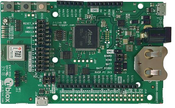
개요
EVK-NINA-B30 development kit은 Nordic Semiconductor nRF52840 Arm Cortex-M4F 기반 NINA-B30x Bluetooth 5.0 module을 지원합니다. Bluetooth Low Energy·IEEE 802.15.4와 USB를 제공합니다.
하드웨어 clock
EVK-NINA-B30x의 NINA-B30x에는 32MHz high-frequency oscillator와 32.768kHz low-frequency oscillator가 내장됩니다.
지원 기능
| Interface | Controller | Driver/Component |
|---|---|---|
| ADC | on-chip | adc |
| CLOCK | on-chip | clock_control |
| FLASH | on-chip | flash |
| GPIO | on-chip | gpio |
| I2C(M) | on-chip | i2c |
| MPU | on-chip | arch/arm |
| NVIC | on-chip | arch/arm |
| PWM | on-chip | pwm |
| RADIO | on-chip | Bluetooth, IEEE 802.15.4 |
| RTC | on-chip | system clock |
| RTT | Segger | console |
| SPI(M/S) | on-chip | spi |
| UART | on-chip | serial |
| USB | on-chip | usb |
| WDT | on-chip | watchdog |
표에 없는 기능은 아직 enable되지 않았습니다.
연결과 I/O
LED
- LED0 red P0.13
- LED1 green P0.25
- LED2 blue P1.00
Push buttons
- BUTTON1 SW1 P0.25
- BUTTON2 SW2 P0.2
- BOOT SW0 boot/reset
Pin 번호는 EVK-NINA-B30x 각 header의 pin 1 marking 기준입니다.
Power (J1)
| PIN # | Signal Name | NINA-B30x Functions |
|---|---|---|
| 1 | N/C | N/A |
| 2 | VDD_IO | N/A |
| 3 | RESET | P0.18 / RESET |
| 4 | 3V3 | N/A |
| 5 | 5V0 | N/A |
| 6 | GND | N/A |
| 7 | GND | N/A |
| 8 | VIN | N/A |
Analog in (J2)
| PIN # | Signal Name | NINA-B30x Functions |
|---|---|---|
| 1 | A0 | P0.04 / AIN2 |
| 2 | A1 | P0.30 / AIN6 |
| 3 | A2 | P0.05 / AIN3 |
| 4 | A3 | P0.02 / AIN0 |
| 5 | A4 | P0.28 / AIN4 |
| 6 | A5 | P0.03 / AIN1 |
Digital I/O (J3)
| PIN # | Signal Name | NINA-B30x Functions |
|---|---|---|
| 8 | D7 | P0.10 |
| 7 | D6 | P0.09 |
| 6 | D5 | P0.11 |
| 5 | D4 | P0.13 |
| 4 | D3 | P0.31 |
| 3 | D2 | P1.12 |
| 2 | D1 (TX) | P1.13 |
| 1 | D0 (RX) | P0.29 |
Digital I/O (J4)
| PIN # | Signal Name | NINA-B30x Functions |
|---|---|---|
| 10 | SCL | P0.24 |
| 9 | SDA | P0.16 |
| 8 | N/C | N/A |
| 7 | GND | N/A |
| 6 | D13 (SCK) | P0.07 |
| 5 | D12 (MISO) | P1.00 |
| 4 | D11 (MOSI) | P0.15 |
| 3 | D10 (SS) | P0.14 |
| 2 | D9 | P0.12 |
| 1 | D8 | P1.09 |
Programming과 debugging
일반 방식으로 build·flash할 수 있지만 원문은 standard debugging target이 현재 제공되지 않는다고 명시합니다.
Flash
Terminal을 열고 Linux에서는 보통 /dev/ttyACM0에서 115200 baud로 출력합니다.
$ minicom -D <tty_device> -b 115200west build -b ubx_evkninab3/nrf52840 samples/hello_world
west flashDebug
Nordic Semiconductor chip과 Segger IC를 사용하는 board debug는 Zephyr Nordic Segger 안내를 따릅니다.
LED와 button 시험
samples/basic/blinky
samples/basic/button
Button과 LED 정의는 boards/u-blox/ubx_evkninab3/ubx_evkninab3_nrf52840.dts에 있습니다.
UART1 사용
Peripheral 연결에 UART가 하나 더 필요하면 application main directory에 overlay를 추가합니다. P0.16은 RX, P0.14는 TX이며 CONFIG_PM_DEVICE=y에서는 sleep pinctrl이 필요합니다.
&pinctrl {
   uart1_default: uart1_default {
      group1 {
         psels = <NRF_PSEL(UART_TX, 0, 14)>,
                 <NRF_PSEL(UART_RX, 0, 16)>;
      };
   };
   /* required if CONFIG_PM_DEVICE=y */
   uart1_sleep: uart1_sleep {
      group1 {
         psels = <NRF_PSEL(UART_TX, 0, 14)>,
                 <NRF_PSEL(UART_RX, 0, 16)>;
         low-power-enable;
      };
   };
};

&uart1 {
  compatible = "nordic,nrf-uarte";
  current-speed = <115200>;
  status = "okay";
  pinctrl-0 = <&uart1_default>;
  pinctrl-1 = <&uart1_sleep>;
  pinctrl-names = "default", "sleep";
};DEVICE_DT_GET(DT_NODELABEL(uart1))로 UART1을 얻습니다. 자동 탐색하려면 <board>.overlay라는 이름으로 application main directory에 둡니다.
Pin 선택
NINA-B3 data sheet section 3의 pin definition에서 GPIO_xx로 표시된 pin을 선택합니다. Radio-sensitive 또는 low-frequency-only pin은 10kHz 미만에서만 사용해야 하므로 UART 115200에 적합하지 않습니다. Pin은 module pad 번호가 아니라 nRF52 pin 번호로 정의합니다.
참고 자료
Source
출처
영어 원문에는 문단, 문서 지시문, 표, 코드, 코드 심벌, 경로를 그대로 보존했습니다.