Part 1
요약·해설
두 Cortex-M33 core, app/net table 25행, IDAU·SPU, read-back protection 복구와 external J-Link 절차를 설명합니다.
nRF5340 · dual Cortex-M33
128 MHz application · 64 MHz network
Armv8-M · IDAU · SPU · secure boot
Part 2
접을 수 있는 영어 원문 전체
영어 원문 전체 펼치기
3D44F7141C13985DB5C5E24EAAC22D6E0C089C6EA5A9D953BB632F2CC41DD39A
.. _raytac_mdbt53_db_40_nrf5340:

Raytac MDBT53-DB-40
###################

Overview
********

Raytac MDBT53-DB-40 demo board is a development board based on the Raytac MDBT53-1M module,
using Nordic Semiconductor nRF5340 ARM Cortex-M33 SoC. Its design concept is to connect all
of the module's pins to 2.54mm pin headers. It is convenient for developers to verify whether
the modules are connected to other peripheral devices or sensors as a tool for software development.

The nRF5340 inside the MDBT53-1M module is a
dual-core SoC based on the Arm® Cortex®-M33 architecture, with:

* a full-featured Arm Cortex-M33F core with DSP instructions, FPU, and
  Armv8-M Security Extension, running at up to 128 MHz, referred to as
  the **application core**
* a secondary Arm Cortex-M33 core, with a reduced feature set, running
  at a fixed 64 MHz, referred to as the **network core**.

The ``raytac_mdbt53_db_40/nrf5340/cpuapp`` build target provides support for the application
core on the nRF5340 SoC. The ``raytac_mdbt53_db_40/nrf5340/cpuapp`` build target provides
support for the network core on the nRF5340 SoC.

nRF5340 SoC provides support for the following devices:

* :abbr:`ADC (Analog to Digital Converter)`
* CLOCK
* FLASH
* :abbr:`GPIO (General Purpose Input Output)`
* :abbr:`IDAU (Implementation Defined Attribution Unit)`
* :abbr:`I2C (Inter-Integrated Circuit)`
* :abbr:`MPU (Memory Protection Unit)`
* :abbr:`NVIC (Nested Vectored Interrupt Controller)`
* :abbr:`PWM (Pulse Width Modulation)`
* :abbr:`QSPI (Quad Serial Peripheral Interface)`
* RADIO (Bluetooth Low Energy and 802.15.4)
* :abbr:`RTC (nRF RTC System Clock)`
* Segger RTT (RTT Console)
* :abbr:`SPI (Serial Peripheral Interface)`
* :abbr:`UARTE (Universal asynchronous receiver-transmitter)`
* :abbr:`WDT (Watchdog Timer)`

.. figure:: ../../../../../../../boards/raytac/mdbt53_db_40/doc/img/MDBT53-DB-40.jpg
     :width: 442px
     :align: center
     :alt: MDBT53-DB-40

     MDBT53-DB-40 (Credit: Raytac Corporation)

More information about the board can be found at the `MDBT53-DB-40 website`_.
The `MDBT53-DB-40 Specification`_ contains the demo board's datasheet.
The `MDBT53-DB-40 Schematic`_ contains the demo board's schematic.

Hardware
********
- Module Demo Board build by MDBT53-1M
- Nordic nRF5340 SoC Solution
- A recommnded 3rd-party module by Nordic Semiconductor.
- Dual-core Arm® Cortex® M33
- 1MB/256KB Flash Memory; 512kB/ 64kB RAM
- Supports BT5 Long Range Features
- Bluetooth specification v5.2
- Supports Bluetooth Direction Finding & Mesh
- Supports Bluetooth low energy audio
- Certifications: FCC, IC, CE, Telec (MIC), KC, SRRC, NCC, RCM, WPC
- RoHs & Reach Compiant.
- 48 GPIO
- Chip Antenna
- Interfaces: SPI, UART, I2C, I2S, PWM, ADC, NFC, and USB
- Highly flexible multiprotocol SoC ideally suited for Bluetooth® Low Energy, ANT+, Zigbee, Thread (802.15.4) ultra low-power wireless applications.
- 4 User LEDs
- 4 User buttons
- 1 Mini USB connector for power supply
- SWD connector for FW programing
- J-Link interface for FW programing
- UART interface for UART communication

Supported Features
==================

The ``raytac_mdbt53_db_40_nrf5340/cpuapp`` board configuration supports the following
hardware features:

+-----------+------------+----------------------+
| Interface | Controller | Driver/Component     |
+===========+============+======================+
| ADC       | on-chip    | adc                  |
+-----------+------------+----------------------+
| CLOCK     | on-chip    | clock_control        |
+-----------+------------+----------------------+
| FLASH     | on-chip    | flash                |
+-----------+------------+----------------------+
| GPIO      | on-chip    | gpio                 |
+-----------+------------+----------------------+
| I2C(M)    | on-chip    | i2c                  |
+-----------+------------+----------------------+
| MPU       | on-chip    | arch/arm             |
+-----------+------------+----------------------+
| NVIC      | on-chip    | arch/arm             |
+-----------+------------+----------------------+
| QSPI(M)   | on-chip    | nor                  |
+-----------+------------+----------------------+
| PWM       | on-chip    | pwm                  |
+-----------+------------+----------------------+
| RTC       | on-chip    | system clock         |
+-----------+------------+----------------------+
| SPI(M/S)  | on-chip    | spi                  |
+-----------+------------+----------------------+
| SPU       | on-chip    | system protection    |
+-----------+------------+----------------------+
| UARTE     | on-chip    | serial               |
+-----------+------------+----------------------+
| WDT       | on-chip    | watchdog             |
+-----------+------------+----------------------+

The ``raytac_mdbt53_db_40_nrf5340/cpunet`` board configuration supports the following
hardware features:

+-----------+------------+----------------------+
| Interface | Controller | Driver/Component     |
+===========+============+======================+
| CLOCK     | on-chip    | clock_control        |
+-----------+------------+----------------------+
| FLASH     | on-chip    | flash                |
+-----------+------------+----------------------+
| GPIO      | on-chip    | gpio                 |
+-----------+------------+----------------------+
| I2C(M)    | on-chip    | i2c                  |
+-----------+------------+----------------------+
| MPU       | on-chip    | arch/arm             |
+-----------+------------+----------------------+
| NVIC      | on-chip    | arch/arm             |
+-----------+------------+----------------------+
| RADIO     | on-chip    | Bluetooth,           |
|           |            | ieee802154           |
+-----------+------------+----------------------+
| RTC       | on-chip    | system clock         |
+-----------+------------+----------------------+
| SPI(M/S)  | on-chip    | spi                  |
+-----------+------------+----------------------+
| UARTE     | on-chip    | serial               |
+-----------+------------+----------------------+
| WDT       | on-chip    | watchdog             |
+-----------+------------+----------------------+

Other hardware features have not been enabled yet for this board.
See `MDBT53-DB-40 website`_ and `MDBT53-DB-40 Specification`_
for a complete list of Raytac MDBT53-DB-40 board hardware features.

Connections and IOs
===================

LED
---

* LED1 (green) = P0.28
* LED2 (red) = P0.30
* LED3 = P0.31
* LED4 = P0.29

Push buttons
------------

* BUTTON1 = SW1 = P0.24
* BUTTON2 = SW2 = P0.08
* BUTTON3 = SW3 = P0.23
* BUTTON4 = SW4 = P0.09

UART
----
* RX = P0.22
* TX = P0.20
* RTS = P0.19
* CTS = P0.21


Security components
===================

- Implementation Defined Attribution Unit (`IDAU`_) on the application core.
  The IDAU is implemented with the System Protection Unit and is used to
  define secure and non-secure memory maps.  By default, all of the memory
  space  (Flash, SRAM, and peripheral address space) is defined to be secure
  accessible only.
- Secure boot.

Programming and Debugging
*************************

nRF5340 application core supports the Armv8-M Security Extension.
Applications built for the ``raytac_mdbt53_db_40/nrf5340/cpuapp`` board by
default boot in the Secure state.

nRF5340 network core does not support the Armv8-M Security Extension.
nRF5340 IDAU may configure bus accesses by the nRF5340 network core
to have Secure attribute set; the latter allows to build and run
Secure only applications on the nRF5340 SoC.

Applications for the ``raytac_mdbt53_db_40_nrf5340`` board configuration can be
built, flashed, and debugged in the usual way. See :ref:`build_an_application` and
:ref:`application_run` for more details on building and running.

.. note::
   Flashing and Debugging Zephyr onto the raytac_mdbt53_db_40_nrf5340 board
   requires an	external J-Link programmer. The programmer is attached to the J1
   or J9 SWD connector.


Flashing
========

Follow the instructions in the :ref:`nordic_segger` page to install
and configure all the necessary software. Further information can be
found in :ref:`nordic_segger_flashing`. Then build and flash
applications as usual (see :ref:`build_an_application` and
:ref:`application_run` for more details).

.. warning::

   The nRF5340 has a flash read-back protection feature. When flash read-back
   protection is active, you will need to recover the chip before reflashing.
   If you are flashing with :ref:`west <west-build-flash-debug>`, run
   this command for more details on the related ``--recover`` option:

Here is an example for the :ref:`hello_world` application.

Use a USB to TTL converter to connect the computer and raytac_mdbt53_db_40_nrf5340
J10 connector. Then run your favorite terminal program to listen for output.

.. code-block:: console

   $ minicom -D <tty_device> -b 115200

Replace :code:`<tty_device>` with the port where the USB to TTL converter
can be found. For example, under Linux, :code:`/dev/ttyUSB0`.

Then build and flash the application in the usual way.

.. zephyr-app-commands::
   :zephyr-app: samples/hello_world
   :board: raytac_mdbt53_db_40_nrf5340
   :goals: build flash

Debugging
=========

The ``raytac_mdbt53_db_40_nrf5340`` board does not have an on-board-J-Link debug IC,
however, instructions from the :ref:`nordic_segger` page also apply to this board.
Use the Debug out connector of nRF52x DK to connect to the J1 connector, and use SEGGER
J-Link OB IF to debug.

Refer to the :ref:`nordic_segger` page to learn about debugging Nordic
boards with a Segger IC.


References
**********

.. _IDAU:
   https://developer.arm.com/docs/100690/latest/attribution-units-sau-and-idau
.. _MDBT53-DB-40 website:
	https://www.raytac.com/product/ins.php?index_id=139
.. _MDBT53-DB-40 Specification:
	https://www.raytac.com/download/index.php?index_id=60
.. _MDBT53-DB-40 Schematic:
	https://www.raytac.com/upload/catalog_b/8b5e364600a9cc8c53a869733e97f07e.jpg
.. _J-Link Software and documentation pack:
	https://www.segger.com/jlink-software.html
Part 3
한국어 전문 번역
개요
Raytac MDBT53-DB-40 demo board는 Nordic Semiconductor nRF5340 ARM Cortex-M33 SoC를 사용하는 Raytac MDBT53-1M module 기반 development board입니다. Module의 모든 pin을 2.54 mm pin header로 연결하는 설계이므로 software development 과정에서 module과 peripheral 또는 sensor의 연결을 검증하기 편리합니다.
MDBT53-1M 안의 nRF5340은 Arm® Cortex®-M33 architecture 기반 dual-core SoC입니다.
- DSP instruction, FPU, Armv8-M Security Extension을 갖추고 최대 128 MHz로 동작하는 full-featured Arm Cortex-M33F application core
- 기능을 줄이고 고정 64 MHz로 동작하는 secondary Arm Cortex-M33 network core
raytac_mdbt53_db_40/nrf5340/cpuapp build target은 nRF5340 application core를 지원합니다. 원문은 같은 raytac_mdbt53_db_40/nrf5340/cpuapp target이 network core도 지원한다고 기술합니다.
nRF5340 SoC는 다음 장치를 지원합니다.
- ADC (Analog-to-Digital Converter)
- CLOCK
- FLASH
- GPIO (General Purpose Input/Output)
- IDAU (Implementation Defined Attribution Unit)
- I2C (Inter-Integrated Circuit)
- MPU (Memory Protection Unit)
- NVIC (Nested Vectored Interrupt Controller)
- PWM (Pulse Width Modulation)
- QSPI (Quad Serial Peripheral Interface)
- RADIO (Bluetooth Low Energy 및 802.15.4)
- RTC (nRF RTC system clock)
- SEGGER RTT (RTT console)
- SPI (Serial Peripheral Interface)
- UARTE (Universal asynchronous receiver-transmitter)
- WDT (Watchdog Timer)
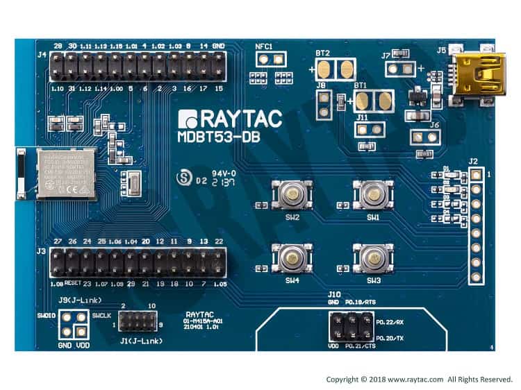
보드 정보는 MDBT53-DB-40 website에서 확인할 수 있습니다. MDBT53-DB-40 specification에는 demo board datasheet가, MDBT53-DB-40 schematic에는 회로도가 있습니다.

하드웨어
- MDBT53-1M으로 만든 module demo board
- Nordic nRF5340 SoC solution
- Nordic Semiconductor가 권장하는 third-party module
- Dual-core Arm® Cortex®-M33
- Application/network core별 1 MB/256 KB flash memory와 512 KB/64 KB RAM
- Bluetooth 5 Long Range feature 지원
- Bluetooth specification v5.2
- Bluetooth Direction Finding 및 Mesh 지원
- Bluetooth Low Energy Audio 지원
- FCC, IC, CE, Telec(MIC), KC, SRRC, NCC, RCM, WPC 인증
- RoHS 및 REACH 준수
- 48 GPIO
- Chip antenna
- SPI, UART, I2C, I2S, PWM, ADC, NFC, USB interface
- Bluetooth® Low Energy, ANT+, Zigbee, Thread(802.15.4) 초저전력 wireless application에 적합한 유연한 multiprotocol SoC
- 4 user LED
- 4 user button
- 전원 공급용 Mini USB connector 1개
- Firmware programming용 SWD connector
- Firmware programming용 J-Link interface
- UART 통신용 UART interface
지원 기능
raytac_mdbt53_db_40/nrf5340/cpuapp board configuration은 다음 hardware feature를 지원합니다.
| 인터페이스 | 컨트롤러 | 드라이버/컴포넌트 |
|---|---|---|
ADC | on-chip | adc |
CLOCK | on-chip | clock_control |
FLASH | on-chip | flash |
GPIO | on-chip | gpio |
I2C(M) | on-chip | i2c |
MPU | on-chip | arch/arm |
NVIC | on-chip | arch/arm |
QSPI(M) | on-chip | nor |
PWM | on-chip | pwm |
RTC | on-chip | system clock |
SPI(M/S) | on-chip | spi |
SPU | on-chip | system protection |
UARTE | on-chip | serial |
WDT | on-chip | watchdog |
raytac_mdbt53_db_40_nrf5340/cpunet board configuration은 다음 hardware feature를 지원합니다.
| 인터페이스 | 컨트롤러 | 드라이버/컴포넌트 |
|---|---|---|
CLOCK | on-chip | clock_control |
FLASH | on-chip | flash |
GPIO | on-chip | gpio |
I2C(M) | on-chip | i2c |
MPU | on-chip | arch/arm |
NVIC | on-chip | arch/arm |
RADIO | on-chip | Bluetooth, ieee802154 |
RTC | on-chip | system clock |
SPI(M/S) | on-chip | spi |
UARTE | on-chip | serial |
WDT | on-chip | watchdog |
그 밖의 hardware feature는 아직 이 보드에서 활성화되지 않았습니다. 전체 목록은 MDBT53-DB-40 website와 MDBT53-DB-40 specification을 참고합니다.
연결과 I/O
LED
- LED1(green) = P0.28
- LED2(red) = P0.30
- LED3 = P0.31
- LED4 = P0.29
Push button
- BUTTON1 = SW1 = P0.24
- BUTTON2 = SW2 = P0.08
- BUTTON3 = SW3 = P0.23
- BUTTON4 = SW4 = P0.09
UART
- RX = P0.22
- TX = P0.20
- RTS = P0.19
- CTS = P0.21
보안 컴포넌트
- Application core의 Implementation Defined Attribution Unit(IDAU). IDAU는 System Protection Unit으로 구현되며 secure/non-secure memory map을 정의합니다. 기본적으로 flash, SRAM, peripheral address space를 포함한 전체 memory space는 secure access 전용입니다.
- Secure boot
프로그래밍과 디버깅
nRF5340 application core는 Armv8-M Security Extension을 지원합니다. raytac_mdbt53_db_40/nrf5340/cpuapp board용으로 build한 application은 기본적으로 Secure state에서 boot합니다.
nRF5340 network core는 Armv8-M Security Extension을 지원하지 않습니다. 그러나 nRF5340 IDAU가 network core의 bus access에 Secure attribute를 설정할 수 있으므로 nRF5340 SoC에서 Secure-only application을 build하고 실행할 수 있습니다.
raytac_mdbt53_db_40_nrf5340 board configuration용 application은 일반적인 방법으로 build, flash, debug할 수 있습니다.
플래시
Zephyr Nordic SEGGER 문서에 따라 필요한 software를 설치하고 구성한 뒤 application을 build하고 flash합니다.
다음은 hello_world 예입니다. USB-to-TTL converter로 computer와 raytac_mdbt53_db_40_nrf5340의 J10 connector를 연결하고 terminal program으로 출력을 수신합니다.
$ minicom -D <tty_device> -b 115200<tty_device>는 USB-to-TTL converter가 나타나는 port입니다. Linux에서는 예를 들어 /dev/ttyUSB0입니다. 그런 다음 application을 build하고 flash합니다.
west build -b raytac_mdbt53_db_40_nrf5340 samples/hello_world
west flash
디버깅
raytac_mdbt53_db_40_nrf5340 board에는 on-board J-Link debug IC가 없지만 Zephyr Nordic SEGGER 지침을 적용할 수 있습니다. nRF52x DK의 Debug out connector를 J1 connector에 연결하고 SEGGER J-Link OB interface로 debug합니다. Nordic 보드를 SEGGER IC로 debug하는 방법은 Zephyr Nordic SEGGER 문서를 참고합니다.
참고 자료
Source
출처
영어 원문에는 문단, 문서 지시문, 표, 코드, 코드 심벌, 경로를 그대로 보존했습니다.