Part 1
요약·해설
Variant target, STLink pin 4행, boot mode 3행, 기능 9종과 서로 다른 LED pin을 담았습니다.
stm32_min_dev@blue · @black
8 MHz HSE · 72 MHz PLL
Blue PC13 · Black PB12
Part 2
접을 수 있는 영어 원문 전체
영어 원문 전체 펼치기
4A186F4F345786C3C039FCB1D02667940E93C2AF9C1D6A5AA3E1A562CDD487AF
.. _stm32_min_dev:

STM32 Minimum Development Board
###############################

Overview
********

The STM32 Minimum Development Board, is a popular and inexpensive
breadboard-friendly breakout board for the `STM32F103x8`_ CPU. There
are two variants of the board:

- Blue Pill Board
- Black Pill Board

Zephyr applications can use the stm32_min_dev@blue or stm32_min_dev@black board
configuration to use these boards.

.. figure:: ../../../../../../../boards/others/stm32_min_dev/doc/img/stm32_min_dev.jpg
     :align: center
     :alt: STM32 Minimum Development Board

     STM32 Minimum Development Board

As the name suggests, these boards have the bare minimum components required to
power on the CPU. For practical use, you'll need to add additional components
and circuits using a breadboard, for example.

Pin Mapping
===========

This port is a starting point for your own customizations and not a complete
port for a specific board. Most of the GPIOs on the STM32 SoC has been exposed
in the external header with silk screen labels that match the SoC's pin names.

Each board vendor has their own variations in pin mapping on their boards'
external connectors and placement of components. Many vendors use port PC13/PB12
for connecting an LED, so only this device is supported by our Zephyr port.
Additional device support is left for the user to implement.

More information on hooking up peripherals and lengthy how to articles can be
found at `EmbedJournal`_.

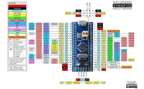
The pinout diagram of STM32 Minimum Development Blue Pill board can be seen
below. The Black Pill's one is similar:

.. figure:: ../../../../../../../boards/others/stm32_min_dev/doc/img/stm32_min_dev_pinout_blue.jpg
     :align: center
     :alt: Pinout for STM32 Minimum Development Blue Pill Board

     Pinout for STM32 Minimum Development Blue Pill Board


STLinkV2 connection:
====================

The board can be flashed by using STLinkV2 with the following connections.

+--------+---------------+
| Pin    | STLINKv2      |
+========+===============+
| G      | GND           |
+--------+---------------+
| CLK    | Clock         |
+--------+---------------+
| IO     | SW IO         |
+--------+---------------+
| V3     | VCC           |
+--------+---------------+

Boot Configuration
==================

The boot configuration for this board is configured through jumpers on B0 (Boot 0)
and B1 (Boot 1). The pins B0 and B1 are present in between logic 0 and 1 lines. The
silk screen on the PCB reads BX- or BX+ to indicate 0 and 1 logic lines for B0 and B1
respectively.

+--------+--------+-------------------+---------------------------------------------+
| Boot 1 | Boot 0 | Boot Mode         | Aliasing                                    |
+========+========+===================+=============================================+
| X      | 0      | Main Flash Memory | Main flash memory is selected as boot space |
+--------+--------+-------------------+---------------------------------------------+
| 0      | 1      | System Memory     | System memory is selected as boot space     |
+--------+--------+-------------------+---------------------------------------------+
| 1      | 1      | Embedded SRAM     | Embedded SRAM is selected as boot space     |
+--------+--------+-------------------+---------------------------------------------+


Supported Features
==================

The stm32_min_dev board configuration supports the following hardware features:

+-----------+------------+----------------------+
| Interface | Controller | Driver/Component     |
+===========+============+======================+
| NVIC      | on-chip    | nested vectored      |
|           |            | interrupt controller |
+-----------+------------+----------------------+
| SYSTICK   | on-chip    | system clock         |
+-----------+------------+----------------------+
| UART      | on-chip    | serial port          |
+-----------+------------+----------------------+
| GPIO      | on-chip    | gpio                 |
+-----------+------------+----------------------+
| I2C       | on-chip    | i2c                  |
+-----------+------------+----------------------+
| PWM       | on-chip    | pwm                  |
+-----------+------------+----------------------+
| SPI       | on-chip    | spi                  |
+-----------+------------+----------------------+
| USB       | on-chip    | USB device           |
+-----------+------------+----------------------+
| ADC       | on-chip    | adc                  |
+-----------+------------+----------------------+

Other hardware features have not been enabled yet for this board.

Connections and IOs
===================

Default Zephyr Peripheral Mapping:
----------------------------------

- UART_1 TX/RX: PA9/PA10
- UART_2 TX/RX: PA2/PA3
- UART_3 TX/RX: PB10/PB11
- I2C_1 SCL/SDA : PB6/PB7
- I2C_2 SCL/SDA : PB10/PB11
- PWM_1_CH1: PA8
- SPI_1 NSS_OE/SCK/MISO/MOSI: PA4/PA5/PA6/PA7
- SPI_2 NSS_OE/SCK/MISO/MOSI: PB12/PB13/PB14/PB15
- USB_DC DM/DP: PA11/PA12
- ADC_1: PA0

System Clock
------------

The on-board 8Mhz crystal is used to produce a 72Mhz system clock with PLL.

Serial Port
-----------

STM32 Minimum Development Board has 3 U(S)ARTs. The Zephyr console output is
assigned to UART_1. Default settings are 115200 8N1.

On-Board LEDs
-------------

The board has one on-board LED that is connected to PB12/PC13 on the black/blue
variants respectively.

Programming and Debugging
*************************

Applications for the ``stm32_min_dev@(blue|black)`` board configuration can be
built and flashed in the usual way (see :ref:`build_an_application` and
:ref:`application_run` for more details).

Flashing
========

Here is an example for the :zephyr:code-sample:`blinky` application.

.. zephyr-app-commands::
   :zephyr-app: samples/basic/blinky
   :board: stm32_min_dev
   :goals: build flash

Debugging
=========

You can debug an application in the usual way.  Here is an example for the
:ref:`hello_world` application.

.. zephyr-app-commands::
   :zephyr-app: samples/hello_world
   :board: stm32_min_dev
   :maybe-skip-config:
   :goals: debug

.. _STM32F103x8:
        https://www.st.com/resource/en/datasheet/stm32f103c8.pdf
.. _EmbedJournal:
        https://embedjournal.com/tag/stm32-min-dev/
Part 3
한국어 전문 번역
개요
STM32 Minimum Development Board는 STM32F103x8용으로 널리 쓰이는 저렴한 breadboard-friendly breakout board이며 Blue Pill과 Black Pill 두 variant가 있습니다. Zephyr target은 stm32_min_dev@blue와 stm32_min_dev@black입니다.
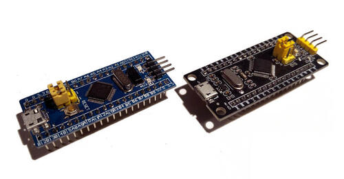
CPU를 켜는 데 필요한 최소 부품만 있으므로 실제 사용에는 breadboard 등의 추가 회로가 필요합니다. 이 port는 특정 board의 완전한 port가 아니라 사용자 customization의 출발점입니다. 대부분 GPIO는 SoC pin name과 같은 silkscreen label로 header에 노출됩니다.
Vendor별 connector mapping과 component 배치는 다릅니다. 많은 board가 LED에 PC13/PB12를 사용하므로 Zephyr port는 이 LED만 지원하며 추가 device는 사용자가 구현해야 합니다.
STLinkV2 연결
| Pin | STLINKv2 |
|---|---|
G | GND |
CLK | Clock |
IO | SW IO |
V3 | VCC |
Boot 구성
B0와 B1 jumper로 설정합니다. PCB silkscreen의 BX-와 BX+는 각각 B0/B1의 logic 0과 1 line을 뜻합니다.
| Boot 1 | Boot 0 | Boot Mode | Aliasing |
|---|---|---|---|
X | 0 | Main Flash Memory | Main flash memory is selected as boot space |
0 | 1 | System Memory | System memory is selected as boot space |
1 | 1 | Embedded SRAM | Embedded SRAM is selected as boot space |
지원 기능
| 인터페이스 | 컨트롤러 | 드라이버/컴포넌트 |
|---|---|---|
NVIC | on-chip | nested vectored interrupt controller |
SYSTICK | on-chip | system clock |
UART | on-chip | serial port |
GPIO | on-chip | gpio |
I2C | on-chip | i2c |
PWM | on-chip | pwm |
SPI | on-chip | spi |
USB | on-chip | USB device |
ADC | on-chip | adc |
표 밖의 기능은 아직 활성화되지 않았습니다.
기본 peripheral mapping
UART_1 TX/RX: PA9/PA10,UART_2: PA2/PA3,UART_3: PB10/PB11I2C_1 SCL/SDA: PB6/PB7,I2C_2: PB10/PB11PWM_1_CH1: PA8SPI_1 NSS/SCK/MISO/MOSI: PA4/PA5/PA6/PA7SPI_2 NSS/SCK/MISO/MOSI: PB12/PB13/PB14/PB15USB_DC DM/DP: PA11/PA12,ADC_1: PA0
Clock, serial, LED
8 MHz crystal과 PLL로 72 MHz system clock을 생성합니다. U(S)ART 3개 중 Zephyr console은 UART_1, 기본값은 115200 8N1입니다. On-board LED는 Black variant에서 PB12, Blue variant에서 PC13입니다.
프로그래밍과 디버깅
stm32_min_dev@(blue|black) target을 일반 방식으로 build·flash합니다.
# Zephyr 저장소 루트에서
west build -b stm32_min_dev@blue samples/basic/blinky
west flash
Debug
# Zephyr 저장소 루트에서
west build -b stm32_min_dev@blue samples/hello_world
west debug
참고 자료
Source
출처
영어 원문에는 문단, 문서 지시문, 표, 코드, 코드 심벌, 경로를 그대로 보존했습니다.