Part 1
요약·해설
지원 기능 4종, connector 92행, 12 MHz HSE와 ARM-USB-OCD-H flash/debug 절차를 담았습니다.
STM32F407ZG · Cortex-M4
12 MHz HSE · up to 168 MHz
Olimex ARM-USB-OCD-H
Part 2
접을 수 있는 영어 원문 전체
영어 원문 전체 펼치기
F1CC7DFC9D654A3ACA4F13CEABE3B89CDACBAD4DE69F6E9BA61B4A0D16711BFF
.. _olimex_stm32_h407:

OLIMEX-STM32-H407
#################

Overview
********

The OLIMEX-STM32-H407 is open source hardware and is based on
the STMicroelectronics STM32F407ZG ARM Cortex-M4 CPU.

.. figure:: ../../../../../../../boards/olimex/stm32_h407/doc/img/olimex_stm32_h407.jpg
     :align: center
     :alt: OLIMEX-STM32-H407

     OLIMEX-STM32-H407

Hardware
********

Information about the board can be found at the
`OLIMEX-STM32-H407 website`_ and `OLIMEX-STM32-H407 user manual`_.
The `ST STM32F407ZG Datasheet`_ contains the processor's
information and the datasheet.

Supported Features
==================

The olimex_stm32_h407 board configuration supports the following
hardware features:

+-----------+------------+----------------------+
| Interface | Controller | Driver/Component     |
+===========+============+======================+
| NVIC      | on-chip    | nested vectored      |
|           |            | interrupt controller |
+-----------+------------+----------------------+
| SYSTICK   | on-chip    | system clock         |
+-----------+------------+----------------------+
| UART      | on-chip    | serial port          |
+-----------+------------+----------------------+
| GPIO      | on-chip    | gpio                 |
+-----------+------------+----------------------+

Other hardware features have not been enabled yet for this board.

Pin Mapping
===========

.. figure:: ../../../../../../../boards/olimex/stm32_h407/doc/img/olimex-stm32-h407-front.jpg
     :align: center
     :alt: OLIMEX-STM32-H407 connectors

     OLIMEX-STM32-H407 connectors

LED
---

* LED (green) = PC13
* PWR_LED (red) = power

Push buttons
------------

* BUT = PA0
* RST = NRST

External Connectors
-------------------

JTAG/SWD debug

+-------+--------------+-------+--------------+
| PIN # | Signal Name  | Pin # | Signal Name  |
+=======+==============+=======+==============+
| 1     | +3.3V        | 11    | -            |
+-------+--------------+-------+--------------+
| 2     | +3.3V        | 12    | GND          |
+-------+--------------+-------+--------------+
| 3     | PB4 / TRST   | 13    | PB3 / TDO    |
+-------+--------------+-------+--------------+
| 4     | GND          | 14    | GND          |
+-------+--------------+-------+--------------+
| 5     | PA15 / TDI   | 15    | PB4 / TRST   |
+-------+--------------+-------+--------------+
| 6     | GND          | 16    | GND          |
+-------+--------------+-------+--------------+
| 7     | PA13 / TMS   | 17    | -            |
+-------+--------------+-------+--------------+
| 8     | GND          | 18    | GND          |
+-------+--------------+-------+--------------+
| 9     | PA14 / TCK   | 19    | +5V_JTAG     |
+-------+--------------+-------+--------------+
| 10    | GND          | 20    | GND          |
+-------+--------------+-------+--------------+

UEXT

+-------+-----------------------+----------------+
| PIN # | Wire   Name           | STM32F407 port |
+=======+=======================+================+
| 1     | +3.3V                 | -              |
+-------+-----------------------+----------------+
| 2     | GND                   | -              |
+-------+-----------------------+----------------+
| 3     | PC6/USART6_TX         | PC6            |
+-------+-----------------------+----------------+
| 4     | PC7/USART6_RX         | PC7            |
+-------+-----------------------+----------------+
| 5     | PB8/I2C1_SCL          | PB8            |
+-------+-----------------------+----------------+
| 6     | PB9/I2C1_SDA          | PB9            |
+-------+-----------------------+----------------+
| 7     | PC2/SPI2_MISO         | PC2            |
+-------+-----------------------+----------------+
| 8     | PC3/SPI2_MOSI         | PC3            |
+-------+-----------------------+----------------+
| 9     | PB10/SPI_SCK/UART3_TX | PB10           |
+-------+-----------------------+----------------+
| 10    | RB7/UEXT_CS           | PB7            |
+-------+-----------------------+----------------+

Arduino Headers
---------------

CON1 power

+-------+--------------+-------------------------+
| Pin   | Signal Name  | STM32F407 Pin#          |
+=======+==============+=========================+
| RST   | RESET        | 25                      |
+-------+--------------+-------------------------+
| 3V3   | VCC (3V3)    | N/A                     |
+-------+--------------+-------------------------+
| 5V    | VDD (5V)     | N/A                     |
+-------+--------------+-------------------------+
| GND   | GND          | N/A                     |
+-------+--------------+-------------------------+
| GND   | GND          | N/A                     |
+-------+--------------+-------------------------+
| VIN   | VIN          | N/A                     |
+-------+--------------+-------------------------+

CON2 analog

+-------+--------------+-------------------------+
| Pin   | Signal Name  | STM32F407 Pin#          |
+=======+==============+=========================+
| A0    | PC0          | 26                      |
+-------+--------------+-------------------------+
| A1    | PC1          | 27                      |
+-------+--------------+-------------------------+
| A2    | PB0          | 46                      |
+-------+--------------+-------------------------+
| A3    | PB1          | 47                      |
+-------+--------------+-------------------------+
| A4    | PC4          | 44                      |
+-------+--------------+-------------------------+
| A5    | PC5          | 45                      |
+-------+--------------+-------------------------+

CON3 digital

+-------+---------------+-------------------------+
| Pin   | Signal Name   | STM32F407 Pin#          |
+=======+===============+=========================+
| D0    | PA3/USART2_RX | 37                      |
+-------+---------------+-------------------------+
| D1    | PA2/USART2_TX | 36                      |
+-------+---------------+-------------------------+
| D2    | PG7           | 92                      |
+-------+---------------+-------------------------+
| D3    | PG8           | 93                      |
+-------+---------------+-------------------------+
| D4    | PG12          | 127                     |
+-------+---------------+-------------------------+
| D5    | PG13          | 128                     |
+-------+---------------+-------------------------+
| D6    | PG14          | 129                     |
+-------+---------------+-------------------------+
| D7    | PG15          | 132                     |
+-------+---------------+-------------------------+

CON4 digital

+-------+--------------+-------------------------+
| Pin   | Signal Name  | STM32F407 Pin#          |
+=======+==============+=========================+
| D8    | PA1          | 35                      |
+-------+--------------+-------------------------+
| D9    | PB11         | 70                      |
+-------+--------------+-------------------------+
| D10   | PA4          | 40                      |
+-------+--------------+-------------------------+
| D11   | PA7          | 43                      |
+-------+--------------+-------------------------+
| D12   | PA6          | 42                      |
+-------+--------------+-------------------------+
| D13   | PA5          | 41                      |
+-------+--------------+-------------------------+
| GND   | AGND         | 31                      |
+-------+--------------+-------------------------+
| AREF  | AREF         | 32                      |
+-------+--------------+-------------------------+

PD

+-------+--------------+-------+--------------+
| PIN # | Signal Name  | Pin # | Signal Name  |
+=======+==============+=======+==============+
| 1     | +3.3V        | 11    | PD8          |
+-------+--------------+-------+--------------+
| 2     | GND          | 12    | PD9          |
+-------+--------------+-------+--------------+
| 3     | PD0          | 13    | PD10         |
+-------+--------------+-------+--------------+
| 4     | PD1          | 14    | PD11         |
+-------+--------------+-------+--------------+
| 5     | PD2/SD_CMD   | 15    | PD12         |
+-------+--------------+-------+--------------+
| 6     | PD3          | 16    | PD13         |
+-------+--------------+-------+--------------+
| 7     | PD4          | 17    | PD14         |
+-------+--------------+-------+--------------+
| 8     | PD5          | 18    | PD15         |
+-------+--------------+-------+--------------+
| 9     | PD6          | 19    | +5V          |
+-------+--------------+-------+--------------+
| 10    | PD7          | 20    | GND          |
+-------+--------------+-------+--------------+

PE

+-------+--------------+-------+--------------+
| PIN # | Signal Name  | Pin # | Signal Name  |
+=======+==============+=======+==============+
| 1     | +3.3V        | 11    | PE8          |
+-------+--------------+-------+--------------+
| 2     | GND          | 12    | PE9          |
+-------+--------------+-------+--------------+
| 3     | PE0          | 13    | PE10         |
+-------+--------------+-------+--------------+
| 4     | PE1          | 14    | PE11         |
+-------+--------------+-------+--------------+
| 5     | PE2          | 15    | PE12         |
+-------+--------------+-------+--------------+
| 6     | PE3          | 16    | PE13         |
+-------+--------------+-------+--------------+
| 7     | PE4          | 17    | PE14         |
+-------+--------------+-------+--------------+
| 8     | PE5          | 18    | PE15         |
+-------+--------------+-------+--------------+
| 9     | PE6          | 19    | +5V          |
+-------+--------------+-------+--------------+
| 10    | PE7          | 20    | GND          |
+-------+--------------+-------+--------------+

PF

+-------+--------------+-------+--------------+
| PIN # | Signal Name  | Pin # | Signal Name  |
+=======+==============+=======+==============+
| 1     | +3.3V        | 11    | PF8          |
+-------+--------------+-------+--------------+
| 2     | GND          | 12    | PF9          |
+-------+--------------+-------+--------------+
| 3     | PF0          | 13    | PF10         |
+-------+--------------+-------+--------------+
| 4     | PF1          | 14    | PF11         |
+-------+--------------+-------+--------------+
| 5     | PF2          | 15    | PF12         |
+-------+--------------+-------+--------------+
| 6     | PF3          | 16    | PF13         |
+-------+--------------+-------+--------------+
| 7     | PF4          | 17    | PF14         |
+-------+--------------+-------+--------------+
| 8     | PF5          | 18    | PF15         |
+-------+--------------+-------+--------------+
| 9     | PF6          | 19    | +5V          |
+-------+--------------+-------+--------------+
| 10    | PF7          | 20    | GND          |
+-------+--------------+-------+--------------+

PG

+-------+--------------+-------+--------------+
| PIN # | Signal Name  | Pin # | Signal Name  |
+=======+==============+=======+==============+
| 1     | +3.3V        | 11    | PG8/D3       |
+-------+--------------+-------+--------------+
| 2     | GND          | 12    | PG9          |
+-------+--------------+-------+--------------+
| 3     | PG0          | 13    | PG10         |
+-------+--------------+-------+--------------+
| 4     | PG1          | 14    | PG11         |
+-------+--------------+-------+--------------+
| 5     | PG2          | 15    | PG12/D4      |
+-------+--------------+-------+--------------+
| 6     | PG3          | 16    | PG13/D5      |
+-------+--------------+-------+--------------+
| 7     | PG4          | 17    | PG14/D6      |
+-------+--------------+-------+--------------+
| 8     | PG5          | 18    | PG15/D7      |
+-------+--------------+-------+--------------+
| 9     | PG6          | 19    | +5V          |
+-------+--------------+-------+--------------+
| 10    | PG7/D2       | 20    | GND          |
+-------+--------------+-------+--------------+

System Clock
============

OLIMEX-STM32-H407 has two external oscillators. The frequency of
the slow clock is 32.768 kHz. The frequency of the main clock
is 12 MHz. The processor can setup HSE to drive the master clock,
which can be set as high as 168 MHz.

Programming and Debugging
*************************
The OLIMEX-STM32-H407 board does not include an embedded debug tool
interface. You will need to use ST tools or an external JTAG probe.
In the following examples the Olimex ARM-USB-OCD-H is used.

If you have an external JTAG probe compliant with the default Zephyr OpenOCD
configuration, however, then applications for the ``olimex_stm32_h407`` board
configuration can be built and flashed in the usual way (see
:ref:`build_an_application` and :ref:`application_run` for more details).

Flashing an application to the Olimex-STM32-H407
================================================

Connect the ARM-USB-OCD-H debugger to your host computer and to the JTAG port
of the OLIMEX-STM32-H407 board. Then build and flash an application.

Here is an example for the :ref:`hello_world` application.

.. zephyr-app-commands::
   :zephyr-app: samples/hello_world
   :board: olimex_stm32_h407
   :goals: build flash

Run a serial host program to connect with your board:

.. code-block:: console

   $ minicom -D /dev/ttyUSB0

After resetting the board, you should see the following message:

.. code-block:: console

   ***** BOOTING ZEPHYR OS v1.11.0 - BUILD: Mar 12 2018 03:12:40 *****
   Hello World! arm


Debugging
=========

Provided that you have a JTAG probe, you can debug an application in the usual
way.  Here is an example for the :ref:`hello_world` application.

.. zephyr-app-commands::
   :zephyr-app: samples/hello_world
   :board: olimex_stm32_h407
   :maybe-skip-config:
   :goals: debug

.. _OLIMEX-STM32-H407 website:
   https://www.olimex.com/Products/ARM/ST/STM32-H407/open-source-hardware

.. _OLIMEX-STM32-H407 user manual:
   https://www.olimex.com/Products/ARM/ST/STM32-H407/resources/STM32-H407.pdf

.. _ST STM32F407ZG Datasheet:
   https://www.st.com/resource/en/reference_manual/dm00031020.pdf
Part 3
한국어 전문 번역
개요
OLIMEX-STM32-H407은 open-source hardware이며 STMicroelectronics STM32F407ZG ARM Cortex-M4 CPU 기반입니다.
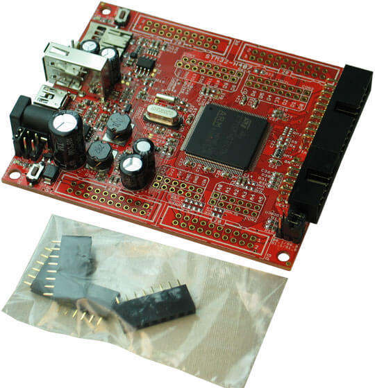
보드 정보는 website와 user manual, processor 정보는 ST STM32F407ZG datasheet에 있습니다.
지원 기능
| 인터페이스 | 컨트롤러 | 드라이버/컴포넌트 |
|---|---|---|
NVIC | on-chip | nested vectored interrupt controller |
SYSTICK | on-chip | system clock |
UART | on-chip | serial port |
GPIO | on-chip | gpio |
표에 없는 하드웨어 기능은 아직 활성화되지 않았습니다.
핀 배치
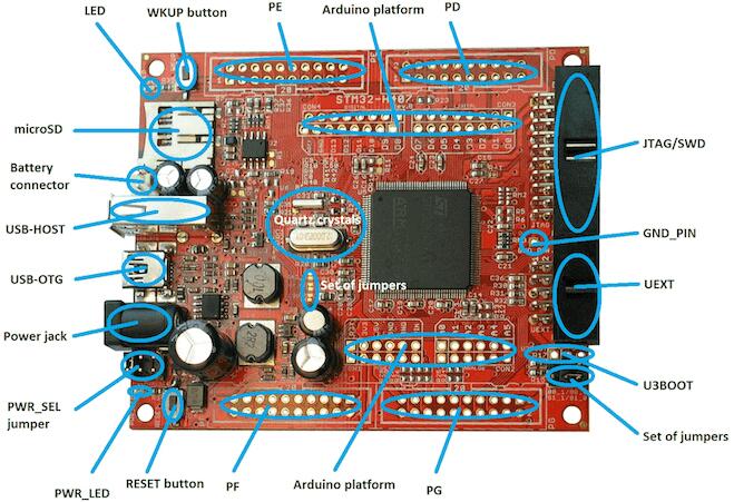
LED와 button
- LED (green):
PC13 - PWR_LED (red): power
- BUT:
PA0 - RST:
NRST
JTAG/SWD debug
| PIN # | Signal Name | Pin # | Signal Name |
|---|---|---|---|
1 | +3.3V | 11 | - |
2 | +3.3V | 12 | GND |
3 | PB4 / TRST | 13 | PB3 / TDO |
4 | GND | 14 | GND |
5 | PA15 / TDI | 15 | PB4 / TRST |
6 | GND | 16 | GND |
7 | PA13 / TMS | 17 | - |
8 | GND | 18 | GND |
9 | PA14 / TCK | 19 | +5V_JTAG |
10 | GND | 20 | GND |
UEXT
| PIN # | Wire Name | STM32F407 port |
|---|---|---|
1 | +3.3V | - |
2 | GND | - |
3 | PC6/USART6_TX | PC6 |
4 | PC7/USART6_RX | PC7 |
5 | PB8/I2C1_SCL | PB8 |
6 | PB9/I2C1_SDA | PB9 |
7 | PC2/SPI2_MISO | PC2 |
8 | PC3/SPI2_MOSI | PC3 |
9 | PB10/SPI_SCK/UART3_TX | PB10 |
10 | RB7/UEXT_CS | PB7 |
Arduino header: CON1 power
| Pin | Signal Name | STM32F407 Pin# |
|---|---|---|
RST | RESET | 25 |
3V3 | VCC (3V3) | N/A |
5V | VDD (5V) | N/A |
GND | GND | N/A |
GND | GND | N/A |
VIN | VIN | N/A |
Arduino header: CON2 analog
| Pin | Signal Name | STM32F407 Pin# |
|---|---|---|
A0 | PC0 | 26 |
A1 | PC1 | 27 |
A2 | PB0 | 46 |
A3 | PB1 | 47 |
A4 | PC4 | 44 |
A5 | PC5 | 45 |
Arduino header: CON3 digital
| Pin | Signal Name | STM32F407 Pin# |
|---|---|---|
D0 | PA3/USART2_RX | 37 |
D1 | PA2/USART2_TX | 36 |
D2 | PG7 | 92 |
D3 | PG8 | 93 |
D4 | PG12 | 127 |
D5 | PG13 | 128 |
D6 | PG14 | 129 |
D7 | PG15 | 132 |
Arduino header: CON4 digital
| Pin | Signal Name | STM32F407 Pin# |
|---|---|---|
D8 | PA1 | 35 |
D9 | PB11 | 70 |
D10 | PA4 | 40 |
D11 | PA7 | 43 |
D12 | PA6 | 42 |
D13 | PA5 | 41 |
GND | AGND | 31 |
AREF | AREF | 32 |
PD connector
| PIN # | Signal Name | Pin # | Signal Name |
|---|---|---|---|
1 | +3.3V | 11 | PD8 |
2 | GND | 12 | PD9 |
3 | PD0 | 13 | PD10 |
4 | PD1 | 14 | PD11 |
5 | PD2/SD_CMD | 15 | PD12 |
6 | PD3 | 16 | PD13 |
7 | PD4 | 17 | PD14 |
8 | PD5 | 18 | PD15 |
9 | PD6 | 19 | +5V |
10 | PD7 | 20 | GND |
PE connector
| PIN # | Signal Name | Pin # | Signal Name |
|---|---|---|---|
1 | +3.3V | 11 | PE8 |
2 | GND | 12 | PE9 |
3 | PE0 | 13 | PE10 |
4 | PE1 | 14 | PE11 |
5 | PE2 | 15 | PE12 |
6 | PE3 | 16 | PE13 |
7 | PE4 | 17 | PE14 |
8 | PE5 | 18 | PE15 |
9 | PE6 | 19 | +5V |
10 | PE7 | 20 | GND |
PF connector
| PIN # | Signal Name | Pin # | Signal Name |
|---|---|---|---|
1 | +3.3V | 11 | PF8 |
2 | GND | 12 | PF9 |
3 | PF0 | 13 | PF10 |
4 | PF1 | 14 | PF11 |
5 | PF2 | 15 | PF12 |
6 | PF3 | 16 | PF13 |
7 | PF4 | 17 | PF14 |
8 | PF5 | 18 | PF15 |
9 | PF6 | 19 | +5V |
10 | PF7 | 20 | GND |
PG connector
| PIN # | Signal Name | Pin # | Signal Name |
|---|---|---|---|
1 | +3.3V | 11 | PG8/D3 |
2 | GND | 12 | PG9 |
3 | PG0 | 13 | PG10 |
4 | PG1 | 14 | PG11 |
5 | PG2 | 15 | PG12/D4 |
6 | PG3 | 16 | PG13/D5 |
7 | PG4 | 17 | PG14/D6 |
8 | PG5 | 18 | PG15/D7 |
9 | PG6 | 19 | +5V |
10 | PG7/D2 | 20 | GND |
System clock
외부 oscillator는 slow clock 32.768 kHz와 main clock 12 MHz 두 개입니다. Processor는 HSE를 master clock source로 설정해 최대 168 MHz로 동작할 수 있습니다.
프로그래밍과 디버깅
Embedded debug interface가 없어 ST 도구나 외부 JTAG probe가 필요합니다. 아래 예는 Olimex ARM-USB-OCD-H를 사용합니다. Zephyr 기본 OpenOCD 구성과 호환되는 외부 JTAG probe가 있다면 olimex_stm32_h407 application을 일반 방식으로 build·flash할 수 있습니다.
Application flash
ARM-USB-OCD-H를 host와 board JTAG port에 연결합니다.
# Zephyr 저장소 루트에서
west build -b olimex_stm32_h407 samples/hello_world
west flash
Serial host program으로 연결합니다.
$ minicom -D /dev/ttyUSB0Reset 후 다음 메시지가 표시됩니다.
***** BOOTING ZEPHYR OS v1.11.0 - BUILD: Mar 12 2018 03:12:40 *****
Hello World! arm
Debug
JTAG probe가 있으면 일반 방식으로 debug할 수 있습니다.
# Zephyr 저장소 루트에서
west build -b olimex_stm32_h407 samples/hello_world
west debug
참고 자료
Source
출처
영어 원문에는 문단, 문서 지시문, 표, 코드, 코드 심벌, 경로를 그대로 보존했습니다.