Part 1
요약·해설
지원 기능 9종, connector 45행, USB power/disconnect 제어와 ST-Link·Olimex·Black Magic probe 선택을 설명합니다.
STM32F103RBT6 · Cortex-M3
UART2 · 115200 8N1
JTAG · SWD · external probe
Part 2
접을 수 있는 영어 원문 전체
영어 원문 전체 펼치기
2227C46605121D60D4287BB1A111F40068F80C25DD3A357CB5A5FBE731AE133C
.. _olimex_stm32_h103:

OLIMEX-STM32-H103
#################

Overview
********

The OLIMEX-STM32-H103 is a simple development board based on the
STMicroelectronics STM32F103RBT6 ARM Cortex-M3 CPU, with all the MCU pins
populated and accessible through two male 26-pin connectors.

.. figure:: ../../../../../../../boards/olimex/stm32_h103/doc/img/olimex_stm32_h103_top.jpg
   :align: center
   :alt: OLIMEX-STM32-H103 top

.. figure:: ../../../../../../../boards/olimex/stm32_h103/doc/img/olimex_stm32_h103_bottom.jpg
   :align: center
   :alt: OLIMEX-STM32-H103 bottom

   OLIMEX-STM32-H103

Hardware
********

Information about the board can be found at the
`OLIMEX-STM32-H103 website`_ and `OLIMEX-STM32-H103 user manual`_.
The `OLIMEX-STM32-H103 schematic`_ is also available.

The `ST STM32F103RB Datasheet`_ contains the processor's
information and the datasheet.

Supported Features
==================

The OLIMEX STM32-H103 supports the following hardware features:

+-----------+------------+----------------------+
| Interface | Controller | Driver/Component     |
+===========+============+======================+
| NVIC      | on-chip    | nested vectored      |
|           |            | interrupt controller |
+-----------+------------+----------------------+
| SYSTICK   | on-chip    | system clock         |
+-----------+------------+----------------------+
| UART      | on-chip    | serial port          |
+-----------+------------+----------------------+
| GPIO      | on-chip    | gpio                 |
+-----------+------------+----------------------+
| I2C       | on-chip    | i2c                  |
+-----------+------------+----------------------+
| PWM       | on-chip    | pwm                  |
+-----------+------------+----------------------+
| SPI       | on-chip    | spi                  |
+-----------+------------+----------------------+
| USB       | on-chip    | USB device           |
+-----------+------------+----------------------+
| ADC       | on-chip    | adc                  |
+-----------+------------+----------------------+

Other hardware features have not been enabled yet for this board.

Connections and IOs
===================

System Clock
------------

The on-board 8 MHz crystal is used to produce a 72 MHz system clock with PLL.

Zephyr Console
--------------

UART2 is used as Zephyr's console. Default settings are 115200 8N1.

On-Board LEDs
-------------

The board has one on-board green LED that is connected to PC12, which
is active low.

There is also a red power LED neither connected nor controlled by the MCU.

On-Board Button
---------------

The board has one user button connected to PA0.

USB
---

USB is not enabled by default.

PC4 can be configured as a GPIO input to detect power on the USB port. It is
possible to disconnect it by desoldering the appropriate pad in the PCB.

PC11 can be used to disconnect the pull-up resistor on the USB-DP line by
setting it high.

External Connectors
-------------------

JTAG/SWD debug

+-------+----------------------+-------+--------------+
| PIN # | Signal Name          | PIN # | Signal Name  |
+=======+======================+=======+==============+
| 1     | TVCC +3.3V           | 2     | TVCC 3.3V    |
+-------+----------------------+-------+--------------+
| 3     | PB4 / TRST           | 4     | GND          |
+-------+----------------------+-------+--------------+
| 5     | PA15 / TDI           | 6     | GND          |
+-------+----------------------+-------+--------------+
| 7     | PA13 / TMS / SWDIO   | 8     | GND          |
+-------+----------------------+-------+--------------+
| 9     | PA14 / TCK / SWCLK   | 10    | GND          |
+-------+----------------------+-------+--------------+
| 11    | NC                   | 12    | GND          |
+-------+----------------------+-------+--------------+
| 13    | PB3 / TDO            | 14    | GND          |
+-------+----------------------+-------+--------------+
| 15    | RST                  | 16    | GND          |
+-------+----------------------+-------+--------------+
| 17    | NC                   | 18    | GND          |
+-------+----------------------+-------+--------------+
| 19    | NC                   | 20    | GND          |
+-------+----------------------+-------+--------------+

EXTENSION 1

+-------+-----------------------+-------+-----------------------+
| PIN # | Name / STM32F103 Port | PIN # | Name / STM32F103 Port |
+=======+=======================+=======+=======================+
| 1     | PA11 / **USB_DM**     | 2     | PA8                   |
+-------+-----------------------+-------+-----------------------+
| 3     | PA12 / **USB_DP**     | 4     | PA9                   |
+-------+-----------------------+-------+-----------------------+
| 5     | +3.3V                 | 6     | GND                   |
+-------+-----------------------+-------+-----------------------+
| 7     | PA10                  | 8     | PC10                  |
+-------+-----------------------+-------+-----------------------+
| 9     | PC11 / **USB_DISC**   | 10    | PC12 / **LED**        |
+-------+-----------------------+-------+-----------------------+
| 11    | PD2                   | 12    | PB5                   |
+-------+-----------------------+-------+-----------------------+
| 13    | PB6                   | 14    | PA6                   |
+-------+-----------------------+-------+-----------------------+
| 15    | PB7                   | 16    | PB8                   |
+-------+-----------------------+-------+-----------------------+
| 17    | PB9                   | 18    | PA5                   |
+-------+-----------------------+-------+-----------------------+
| 19    | PC0                   | 20    | PC1                   |
+-------+-----------------------+-------+-----------------------+
| 21    | PB0                   | 22    | PA7                   |
+-------+-----------------------+-------+-----------------------+
| 23    | VBAT                  | 24    | PC13                  |
+-------+-----------------------+-------+-----------------------+
| 25    | RST                   | 26    | PB1                   |
+-------+-----------------------+-------+-----------------------+

EXTENSION 2

+-------+------------------------+-------+-----------------------+
| PIN # | Name / STM32F103 Port  | PIN # | Name / STM32F103 Port |
+=======+========================+=======+=======================+
| 1     | VDDA                   | 2     | PC2                   |
+-------+------------------------+-------+-----------------------+
| 3     | GNDA                   | 4     | PA0 / **BUTTON**      |
+-------+------------------------+-------+-----------------------+
| 5     | +3.3V                  | 6     | GND                   |
+-------+------------------------+-------+-----------------------+
| 7     | PA2 / **USART2_TX**    | 8     | PA1                   |
+-------+------------------------+-------+-----------------------+
| 9     | PC3                    | 10    | PA3 / **USART2_RX**   |
+-------+------------------------+-------+-----------------------+
| 11    | PA4                    | 12    | PC4 / **USB_POWER**   |
+-------+------------------------+-------+-----------------------+
| 13    | PC5                    | 14    | PB10                  |
+-------+------------------------+-------+-----------------------+
| 15    | P11                    | 16    | PB13                  |
+-------+------------------------+-------+-----------------------+
| 17    | PB12                   | 18    | PB14                  |
+-------+------------------------+-------+-----------------------+
| 19    | PB15                   | 20    | PC6                   |
+-------+------------------------+-------+-----------------------+
| 21    | PC7                    | 22    | PC8                   |
+-------+------------------------+-------+-----------------------+
| 23    | +5V USB                | 24    | PC9                   |
+-------+------------------------+-------+-----------------------+
| 25    | GND                    | 26    | VIN                   |
+-------+------------------------+-------+-----------------------+


Programming and Debugging
*************************

This board does not include any embedded debug tool interface, instead you
will have to use an external probe connected to the available 20-pin JTAG
connector to program and debug the board. Both JTAG and SWD are supported.

By default when using ``west debug`` ST-Link will be used with OpenOCD's
SWD transport, but it is also possible to use JTAG with the Olimex ARM-USB-OCD-H
probe, for instance. For the latter, you should replace the file ``openocd.cfg``
by ``openocd_olimex_jtag.cfg``, located in the board's support directory.

The ``blackmagicprobe`` can also be used to program the device.

Flashing
========

Here is an example for the :zephyr:code-sample:`button` application.

.. zephyr-app-commands::
   :zephyr-app: samples/basic/button
   :board: olimex_stm32_h103
   :goals: build flash

Debugging
=========

You can debug an application in the usual way.  Here is an example for the
:ref:`hello_world` application.

.. zephyr-app-commands::
   :zephyr-app: samples/hello_world
   :board: olimex_stm32_h103
   :maybe-skip-config:
   :goals: debug

References
**********

- `OLIMEX-STM32-H103 website`_
- `OLIMEX-STM32-H103 user manual`_
- `OLIMEX-STM32-H103 schematic`_

.. _OLIMEX-STM32-H103 website:
   https://www.olimex.com/Products/ARM/ST/STM32-H103/

.. _OLIMEX-STM32-H103 user manual:
   https://www.olimex.com/Products/ARM/ST/STM32-H103/resources/STM32-H103.pdf

.. _OLIMEX-STM32-H103 schematic:
   https://www.olimex.com/Products/ARM/ST/STM32-H405/resources/STM32-H405_sch.pdf

.. _ST STM32F103RB Datasheet:
   https://www.st.com/resource/en/datasheet/stm32f103rb.pdf

.. _STM32f103RB:
   https://www.st.com/en/microcontrollers-microprocessors/stm32f103rb.html
Part 3
한국어 전문 번역
개요
OLIMEX-STM32-H103은 STMicroelectronics STM32F103RBT6 ARM Cortex-M3 CPU 기반의 단순한 development board입니다. MCU의 모든 pin이 실장되어 두 개의 male 26-pin connector로 접근할 수 있습니다.
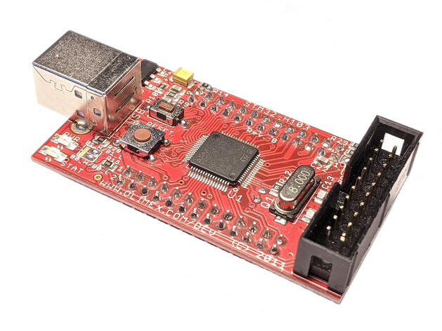
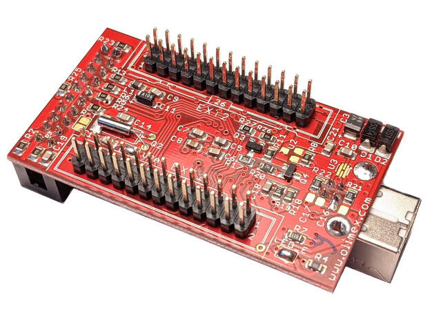
보드 정보는 website, user manual, schematic에서 확인할 수 있고 processor 정보는 ST STM32F103RB datasheet에 있습니다.
지원 기능
| 인터페이스 | 컨트롤러 | 드라이버/컴포넌트 |
|---|---|---|
NVIC | on-chip | nested vectored interrupt controller |
SYSTICK | on-chip | system clock |
UART | on-chip | serial port |
GPIO | on-chip | gpio |
I2C | on-chip | i2c |
PWM | on-chip | pwm |
SPI | on-chip | spi |
USB | on-chip | USB device |
ADC | on-chip | adc |
표에 없는 하드웨어 기능은 아직 활성화되지 않았습니다.
연결과 I/O
System clock
On-board 8 MHz crystal과 PLL로 72 MHz system clock을 생성합니다.
Zephyr console
UART2를 사용하며 기본값은 115200 8N1입니다.
LED와 button
Green LED는 active-low PC12에 연결됩니다. Red power LED는 MCU와 연결되지 않아 MCU가 제어하지 않습니다. User button은 PA0입니다.
USB
USB는 기본 활성화되지 않습니다. PC4를 GPIO input으로 설정해 USB port 전원을 감지할 수 있고 PCB의 해당 pad를 desolder하면 연결을 끊을 수 있습니다. PC11을 high로 설정하면 USB-DP line의 pull-up resistor를 분리할 수 있습니다.
JTAG/SWD debug
| PIN # | Signal Name | PIN # | Signal Name |
|---|---|---|---|
1 | TVCC +3.3V | 2 | TVCC 3.3V |
3 | PB4 / TRST | 4 | GND |
5 | PA15 / TDI | 6 | GND |
7 | PA13 / TMS / SWDIO | 8 | GND |
9 | PA14 / TCK / SWCLK | 10 | GND |
11 | NC | 12 | GND |
13 | PB3 / TDO | 14 | GND |
15 | RST | 16 | GND |
17 | NC | 18 | GND |
19 | NC | 20 | GND |
EXTENSION 1
| PIN # | Name / STM32F103 Port | PIN # | Name / STM32F103 Port |
|---|---|---|---|
1 | PA11 / USB_DM | 2 | PA8 |
3 | PA12 / USB_DP | 4 | PA9 |
5 | +3.3V | 6 | GND |
7 | PA10 | 8 | PC10 |
9 | PC11 / USB_DISC | 10 | PC12 / LED |
11 | PD2 | 12 | PB5 |
13 | PB6 | 14 | PA6 |
15 | PB7 | 16 | PB8 |
17 | PB9 | 18 | PA5 |
19 | PC0 | 20 | PC1 |
21 | PB0 | 22 | PA7 |
23 | VBAT | 24 | PC13 |
25 | RST | 26 | PB1 |
EXTENSION 2
| PIN # | Name / STM32F103 Port | PIN # | Name / STM32F103 Port |
|---|---|---|---|
1 | VDDA | 2 | PC2 |
3 | GNDA | 4 | PA0 / BUTTON |
5 | +3.3V | 6 | GND |
7 | PA2 / USART2_TX | 8 | PA1 |
9 | PC3 | 10 | PA3 / USART2_RX |
11 | PA4 | 12 | PC4 / USB_POWER |
13 | PC5 | 14 | PB10 |
15 | P11 | 16 | PB13 |
17 | PB12 | 18 | PB14 |
19 | PB15 | 20 | PC6 |
21 | PC7 | 22 | PC8 |
23 | +5V USB | 24 | PC9 |
25 | GND | 26 | VIN |
프로그래밍과 디버깅
Embedded debug interface가 없으므로 20-pin JTAG connector에 외부 probe를 연결해야 합니다. JTAG와 SWD를 모두 지원합니다.
west debug 기본값은 ST-Link와 OpenOCD SWD transport입니다. Olimex ARM-USB-OCD-H로 JTAG를 쓸 수도 있으며 이때 board support directory의 openocd.cfg를 openocd_olimex_jtag.cfg로 교체합니다. blackmagicprobe로도 device를 program할 수 있습니다.
Flash
# Zephyr 저장소 루트에서
west build -b olimex_stm32_h103 samples/basic/button
west flash
Debug
# Zephyr 저장소 루트에서
west build -b olimex_stm32_h103 samples/hello_world
west debug
참고 자료
Source
출처
영어 원문에는 문단, 문서 지시문, 표, 코드, 코드 심벌, 경로를 그대로 보존했습니다.