Part 1
요약·해설
CPU0 S/NS·CPU1 target, TF-M·MCUboot partition, dual-core mailbox, TrustZone 수동 flash와 J-Link·LinkServer·DAPLink 경로를 설명합니다.
Dual Cortex-M33 · 100 MHz
TrustZone · TF-M · MCUboot
CPU0/CPU1 · IPC · shared RAM
Part 2
접을 수 있는 영어 원문 전체
영어 원문 전체 펼치기
A2E210DFA56565A2E977177400ADE3F43BCFE8D69B582DECCBCEFF8F60698DF7
.. _lpcxpresso55s69:

NXP LPCXPRESSO55S69
###################

Overview
********

The LPCXpresso55S69 development board provides the ideal platform for evaluation
of and development with the LPC55S6x MCU based on the Arm® Cortex®-M33
architecture. The board includes a high performance onboard debug probe, audio
subsystem, and accelerometer, with several options for adding off-the-shelf
add-on boards for networking, sensors, displays, and other interfaces.

.. image:: ../../../../../../../boards/nxp/lpcxpresso55s69/doc/lpcxpresso55s69.jpg
   :align: center
   :alt: LPCXPRESSO55S69

Hardware
********

- LPC55S69 dual core Arm Cortex-M33 microcontroller running at up to 100 MHz
- Onboard, high-speed USB, Link2 debug probe with CMSIS-DAP and SEGGER J-Link
  protocol options
- UART and SPI port bridging from LPC55S69 target to USB via the onboard debug
  probe
- Hardware support for external debug probe
- 3 x user LEDs, plus Reset, ISP (3) and user buttons
- Micro SD card slot (4-bit SDIO)
- NXP MMA8652FCR1 accelerometer
- Stereo audio codec with line in/out
- High and full speed USB ports with micro A/B connector for host or device
  functionality
- MikroEletronika Click expansion option
- LPCXpresso-V3 expansion option compatible with Arduino UNO
- PMod compatible expansion / host connector

For more information about the LPC55S69 SoC and LPCXPRESSO55S69 board, see:

- `LPC55S69 SoC Website`_
- `LPC55S69 Datasheet`_
- `LPC55S69 Reference Manual`_
- `LPCXPRESSO55S69 Website`_
- `LPCXPRESSO55S69 User Guide`_
- `LPCXPRESSO55S69 Schematics`_
- `LPCXPRESSO55S69 Debug Firmware`_

Supported Features
==================

NXP considers the LPCXpresso55S69 as the superset board for the LPC55xx
series of MCUs.  This board is a focus for NXP's Full Platform Support for
Zephyr, to better enable the entire LPC55xx series.  NXP prioritizes enabling
this board with new support for Zephyr features.  The lpcxpresso55s69 board
configuration supports the following hardware features:

+-----------+------------+-------------------------------------+
| Interface | Controller | Driver/Component                    |
+===========+============+=====================================+
| NVIC      | on-chip    | nested vector interrupt controller  |
+-----------+------------+-------------------------------------+
| SYSTICK   | on-chip    | systick                             |
+-----------+------------+-------------------------------------+
| IOCON     | on-chip    | pinmux                              |
+-----------+------------+-------------------------------------+
| GPIO      | on-chip    | gpio                                |
+-----------+------------+-------------------------------------+
| I2C       | on-chip    | i2c                                 |
+-----------+------------+-------------------------------------+
| SPI       | on-chip    | spi                                 |
+-----------+------------+-------------------------------------+
| USART     | on-chip    | serial port-polling;                |
|           |            | serial port-interrupt               |
+-----------+------------+-------------------------------------+
| WWDT      | on-chip    | windowed watchdog timer             |
+-----------+------------+-------------------------------------+
| TrustZone | on-chip    | Trusted Firmware-M                  |
+-----------+------------+-------------------------------------+
| ADC       | on-chip    | adc                                 |
+-----------+------------+-------------------------------------+
| CLOCK     | on-chip    | clock_control                       |
+-----------+------------+-------------------------------------+
| MAILBOX   | on-chip    | ipm                                 |
+-----------+------------+-------------------------------------+
| HWINFO    | on-chip    | Unique device serial number         |
+-----------+------------+-------------------------------------+
| USB HS    | on-chip    | USB High Speed device               |
+-----------+------------+-------------------------------------+
| USB FS    | on-chip    | USB Full Speed device               |
+-----------+------------+-------------------------------------+
| COUNTER   | on-chip    | counter                             |
+-----------+------------+-------------------------------------+
| I2S       | on-chip    | i2s                                 |
+-----------+------------+-------------------------------------+
| PWM       | on-chip    | pwm                                 |
+-----------+------------+-------------------------------------+
| RNG       | on-chip    | entropy;                            |
|           |            | random                              |
+-----------+------------+-------------------------------------+
| IAP       | on-chip    | flash programming                   |
+-----------+------------+-------------------------------------+
| SDIF      | on-chip    | sdhc                                |
+-----------+------------+-------------------------------------+
| DMA       | on-chip    | dma (on CPU0)                       |
+-----------+------------+-------------------------------------+

Targets available
==================

The default configuration file
:zephyr_file:`boards/nxp/lpcxpresso55s69/lpcxpresso55s69_lpc55s69_cpu0_defconfig`
only enables the first core.
CPU0 is the only target that can run standalone.

- *lpcxpresso55s69/lpc55s69/cpu0* secure (S) address space for CPU0
- *lpcxpresso55s69/lpc55s69/cpu0/ns* non-secure (NS) address space for CPU0
- *lpcxpresso55s69/lpc55s69/cpu1* CPU1 target, no security extensions

NS target for CPU0 does not work correctly without a secure image to configure
the system, then hand execution over to the NS environment. To enable a secure
image, run any of the ``tfm_integration`` samples. When using the NS target
``CONFIG_BUILD_WITH_TFM`` is always enabled to ensure that a valid S image is
included during the build process.

CPU1 does not work without CPU0 enabling it.
To enable it, run one of the following samples in ``subsys\ipc``:

- ``ipm_mcux``
- ``openamp``

Connections and IOs
===================

The LPC55S69 SoC has IOCON registers, which can be used to configure the
functionality of a pin.

+---------+-----------------+----------------------------+
| Name    | Function        | Usage                      |
+=========+=================+============================+
| PIO0_26 | SPI             | SPI MOSI                   |
+---------+-----------------+----------------------------+
| PIO0_27 | USART           | USART TX                   |
+---------+-----------------+----------------------------+
| PIO0_29 | USART           | USART RX                   |
+---------+-----------------+----------------------------+
| PIO0_30 | USART           | USART TX                   |
+---------+-----------------+----------------------------+
| PIO1_1  | SPI             | SPI SSEL                   |
+---------+-----------------+----------------------------+
| PIO1_2  | SPI             | SPI SCK                    |
+---------+-----------------+----------------------------+
| PIO1_3  | SPI             | SPI MISO                   |
+---------+-----------------+----------------------------+
| PIO1_4  | GPIO            | RED LED                    |
+---------+-----------------+----------------------------+
| PIO1_6  | GPIO            | BLUE_LED                   |
+---------+-----------------+----------------------------+
| PIO1_7  | GPIO            | GREEN LED                  |
+---------+-----------------+----------------------------+
| PIO1_20 | I2C             | I2C SCL                    |
+---------+-----------------+----------------------------+
| PIO1_21 | I2C             | I2C SDA                    |
+---------+-----------------+----------------------------+
| PIO1_24 | USART           | USART RX                   |
+---------+-----------------+----------------------------+
| PIO0_20 | I2S             | I2S DATAOUT                |
+---------+-----------------+----------------------------+
| PIO0_19 | I2S             | I2S TX WS                  |
+---------+-----------------+----------------------------+
| PIO0_21 | I2S             | I2S TX SCK                 |
+---------+-----------------+----------------------------+
| PIO1_13 | I2S             | I2S DATAIN                 |
+---------+-----------------+----------------------------+
| PIO0_15 | SCT0_OUT2       | PWM                        |
+---------+-----------------+----------------------------+
| PIO0_24 | SD0_D0          | SDHC                       |
+---------+-----------------+----------------------------+
| PIO0_25 | SD0_D1          | SDHC                       |
+---------+-----------------+----------------------------+
| PIO0_31 | SD0_D2          | SDHC                       |
+---------+-----------------+----------------------------+
| PIO0_7  | SD0_CLK         | SDHC                       |
+---------+-----------------+----------------------------+
| PIO0_8  | SD0_CMD         | SDHC                       |
+---------+-----------------+----------------------------+
| PIO0_9  | SD0_POW_EN      | SDHC                       |
+---------+-----------------+----------------------------+
| PIO1_0  | SD0_D3          | SDHC                       |
+---------+-----------------+----------------------------+

Memory mappings
===============

There are multiple memory configurations, they all start from the
MCUboot partitioning which looks like the table below

+----------+------------------+---------------------------------+
| Name     | Address[Size]    | Comment                         |
+==========+==================+=================================+
| boot     | 0x00000000[32K]  | Bootloader                      |
+----------+------------------+---------------------------------+
| slot0    | 0x00008000[160k] | Image that runs after boot      |
+----------+------------------+---------------------------------+
| slot0_ns | 0x00030000[96k]  | Second image, core 1 or NS      |
+----------+------------------+---------------------------------+
| slot1    | 0x00048000[160k] | Updates slot0 image             |
+----------+------------------+---------------------------------+
| slot1_ns | 0x00070000[96k]  | Updates slot0_ns image          |
+----------+------------------+---------------------------------+
| storage  | 0x00088000[50k]  | File system, persistent storage |
+----------+------------------+---------------------------------+

See below examples of how this partitioning is used

Trusted Execution
*****************

+-----------+------------------+--------------------+
| Memory    | Address[Size]    | Comment            |
+===========+==================+====================+
| MCUboot   | 0x00000000[32K]  | Secure bootloader  |
+-----------+------------------+--------------------+
| TFM_S     | 0x00008000[160k] | Secure image       |
+-----------+------------------+--------------------+
| Zephyr_NS | 0x00030000[96k]  | Non-Secure image   |
+-----------+------------------+--------------------+
| storage   | 0x00088000[50k]  | Persistent storage |
+-----------+------------------+--------------------+

+----------------+------------------+-------------------+
| RAM            | Address[Size]    | Comment           |
+================+==================+===================+
| secure_ram     | 0x20000000[136k] | Secure memory     |
+----------------+------------------+-------------------+
| non_secure_ram | 0x20022000[136k] | Non-Secure memory |
+----------------+------------------+-------------------+

Dual Core samples
*****************

+--------+------------------+----------------------------+
| Memory | Address[Size]    | Comment                    |
+========+==================+============================+
| CPU0   | 0x00000000[630K] | CPU0, can access all flash |
+--------+------------------+----------------------------+
| CPU1   | 0x00030000[96k]  | CPU1, has no MPU           |
+--------+------------------+----------------------------+

+-------+------------------+-----------------------+
| RAM   | Address[Size]    | Comment               |
+=======+==================+=======================+
| sram0 | 0x20000000[64k]  | CPU0 memory           |
+-------+------------------+-----------------------+
| sram3 | 0x20030000[64k]  | CPU1 memory           |
+-------+------------------+-----------------------+
| sram4 | 0x20040000[16k]  | Mailbox/shared memory |
+-------+------------------+-----------------------+

System Clock
============

The LPC55S69 SoC is configured to use PLL1 clocked from the external 16MHz
crystal, running at 144MHz as a source for the system clock. When the flash
controller is enabled, the core clock will be reduced to 96MHz. The application
may reconfigure clocks after initialization, provided that the core clock is
always set to 96MHz when flash programming operations are performed.

Serial Port
===========

The LPC55S69 SoC has 8 FLEXCOMM interfaces for serial communication.  One is
configured as USART for the console and the remaining are not used.

Programming and Debugging
*************************

Build and flash applications as usual (see :ref:`build_an_application` and
:ref:`application_run` for more details).

Configuring a Debug Probe
=========================

A debug probe is used for both flashing and debugging the board. This board is
configured by default to use the LPC-Link2 CMSIS-DAP Onboard Debug Probe,
however the :ref:`pyocd-debug-host-tools` does not yet support this probe so you
must reconfigure the board for one of the following debug probes instead.

:ref:`lpclink2-jlink-onboard-debug-probe`
-----------------------------------------

Install the :ref:`jlink-debug-host-tools` and make sure they are in your search
path.

Follow the instructions in :ref:`lpclink2-jlink-onboard-debug-probe` to program
the J-Link firmware. Please make sure you have the latest firmware for this
board.

:ref:`lpclink2-cmsis-onboard-debug-probe`
-----------------------------------------

        1. Install the :ref:`linkserver-debug-host-tools` and make sure they are in your search path.
        2. To update the debug firmware, please follow the instructions on `LPCXPRESSO55S69 Debug Firmware`

:ref:`opensda-daplink-onboard-debug-probe`
------------------------------------------

PyOCD support for this board is ongoing and not yet available.
To use DAPLink's flash memory programming on this board, follow the instructions
for `updating LPCXpresso firmware`_.

Configuring a Console
=====================

Connect a USB cable from your PC to P6, and use the serial terminal of your choice
(minicom, putty, etc.) with the following settings:

- Speed: 115200
- Data: 8 bits
- Parity: None
- Stop bits: 1

Flashing
========

Here is an example for the :ref:`hello_world` application. This example uses the
:ref:`jlink-debug-host-tools` as default.

.. zephyr-app-commands::
   :zephyr-app: samples/hello_world
   :board: lpcxpresso55s69/lpc55s69/cpu0
   :goals: flash

Open a serial terminal, reset the board (press the RESET button), and you should
see the following message in the terminal:

.. code-block:: console

   ***** Booting Zephyr OS v1.14.0 *****
   Hello World! lpcxpresso55s69

Building and flashing secure/non-secure with Arm |reg| TrustZone |reg|
----------------------------------------------------------------------
The TF-M integration samples can be run using the
``lpcxpresso55s69/lpc55s69/cpu0/ns`` target. To run we need to manually flash
the resulting image (``tfm_merged.hex``) with a J-Link as follows
(reset and erase are for recovering a locked core):

   .. code-block:: console

      JLinkExe -device lpc55s69 -if swd -speed 2000 -autoconnect 1
      J-Link>r
      J-Link>erase
      J-Link>loadfile build/zephyr/tfm_merged.hex

We need to reset the board manually after flashing the image to run this code.

Building a dual-core image
--------------------------
The dual-core samples are run using ``lpcxpresso55s69/lpc55s69/cpu0`` target.
Images built for ``lpcxpresso55s69/lpc55s69/cpu1`` will be loaded from flash
and executed on the second core when ``SECOND_CORE_MCUX`` is selected. For
an example of building for both cores with sysbuild, see
``samples/subsys/ipc/openamp/``

Debugging
=========

Here is an example for the :ref:`hello_world` application. This example uses the
:ref:`jlink-debug-host-tools` as default.

.. zephyr-app-commands::
   :zephyr-app: samples/hello_world
   :board: lpcxpresso55s69/lpc55s69/cpu0
   :goals: debug

Open a serial terminal, step through the application in your debugger, and you
should see the following message in the terminal:

.. code-block:: console

   ***** Booting Zephyr OS zephyr-v1.14.0 *****
   Hello World! lpcxpresso55s69

.. _LPC55S69 SoC Website:
   https://www.nxp.com/products/processors-and-microcontrollers/arm-based-processors-and-mcus/lpc-cortex-m-mcus/lpc5500-cortex-m33/high-efficiency-arm-cortex-m33-based-microcontroller-family:LPC55S6x

.. _LPC55S69 Datasheet:
   https://www.nxp.com/docs/en/nxp/data-sheets/LPC55S6x_DS.pdf

.. _LPC55S69 Reference Manual:
   https://www.nxp.com/webapp/Download?colCode=UM11126

.. _LPCXPRESSO55S69 Website:
   https://www.nxp.com/products/processors-and-microcontrollers/arm-based-processors-and-mcus/lpc-cortex-m-mcus/lpc5500-cortex-m33/lpcxpresso55s69-development-board:LPC55S69-EVK

.. _LPCXPRESSO55S69 User Guide:
   https://www.nxp.com/webapp/Download?colCode=UM11158

.. _LPCXPRESSO55S69 Debug Firmware:
   https://www.nxp.com/docs/en/application-note/AN13206.pdf

.. _LPCXPRESSO55S69 Schematics:
   https://www.nxp.com/webapp/Download?colCode=LPC55S69-SCH

.. _updating LPCXpresso firmware:
   https://os.mbed.com/teams/NXP/wiki/Updating-LPCXpresso-firmware
Part 3
한국어 전문 번역
개요
LPCXpresso55S69 개발 보드는 Arm Cortex-M33 기반 LPC55S6x MCU 평가·개발 플랫폼입니다. 고성능 온보드 디버그 프로브, audio subsystem, accelerometer와 네트워크·센서·디스플레이 확장 옵션을 제공합니다.
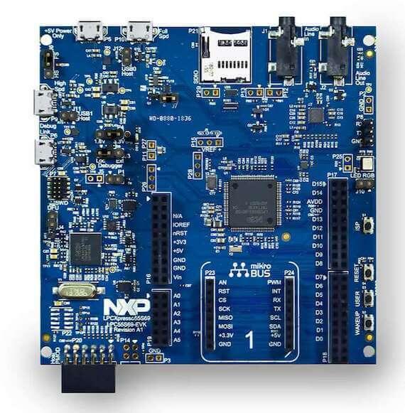
하드웨어
- 최대 100 MHz LPC55S69 dual-core Cortex-M33
- CMSIS-DAP/J-Link 선택형 온보드 고속 USB Link2 프로브와 외부 프로브 지원
- UART·SPI USB bridge
- 사용자 LED 3개와 Reset·ISP(3)·user 버튼
- 4-bit SDIO microSD
- MMA8652FCR1 accelerometer와 stereo audio codec
- micro A/B High/Full-Speed USB host/device
- Click, Arduino UNO 호환 LPCXpresso-V3, PMod 확장
지원 기능
NXP는 LPCXpresso55S69를 LPC55xx 전체 계열의 상위 집합 보드로 보고 Zephyr Full Platform Support와 새 기능을 우선 활성화합니다.
| 인터페이스 | 컨트롤러 | 드라이버/컴포넌트 |
|---|---|---|
NVIC | on-chip | nested vector interrupt controller |
SYSTICK | on-chip | systick |
IOCON | on-chip | pinmux |
GPIO | on-chip | gpio |
I2C | on-chip | i2c |
SPI | on-chip | spi |
USART | on-chip | serial port-polling; serial port-interrupt |
WWDT | on-chip | windowed watchdog timer |
TrustZone | on-chip | Trusted Firmware-M |
ADC | on-chip | adc |
CLOCK | on-chip | clock_control |
MAILBOX | on-chip | ipm |
HWINFO | on-chip | Unique device serial number |
USB HS | on-chip | USB High Speed device |
USB FS | on-chip | USB Full Speed device |
COUNTER | on-chip | counter |
I2S | on-chip | i2s |
PWM | on-chip | pwm |
RNG | on-chip | entropy; random |
IAP | on-chip | flash programming |
SDIF | on-chip | sdhc |
DMA | on-chip | dma (on CPU0) |
사용 가능한 target
기본 lpcxpresso55s69_lpc55s69_cpu0_defconfig는 첫 코어만 활성화하며 CPU0만 독립 실행할 수 있습니다.
lpcxpresso55s69/lpc55s69/cpu0: CPU0 secure(S) 주소 공간lpcxpresso55s69/lpc55s69/cpu0/ns: CPU0 non-secure(NS) 주소 공간lpcxpresso55s69/lpc55s69/cpu1: security extension 없는 CPU1
CPU0 NS target은 시스템을 구성하고 NS로 넘기는 secure image 없이는 올바르게 동작하지 않습니다. tfm_integration 샘플을 사용하며 NS target에서는 CONFIG_BUILD_WITH_TFM이 항상 활성화되어 유효한 S image를 포함합니다. CPU1은 CPU0이 활성화해야 하며 subsys/ipc의 ipm_mcux 또는 openamp 샘플을 사용합니다.
연결과 I/O
IOCON 레지스터로 핀 기능을 구성합니다.
| 이름 | 기능 | 용도 |
|---|---|---|
PIO0_26 | SPI | SPI MOSI |
PIO0_27 | USART | USART TX |
PIO0_29 | USART | USART RX |
PIO0_30 | USART | USART TX |
PIO1_1 | SPI | SPI SSEL |
PIO1_2 | SPI | SPI SCK |
PIO1_3 | SPI | SPI MISO |
PIO1_4 | GPIO | RED LED |
PIO1_6 | GPIO | BLUE_LED |
PIO1_7 | GPIO | GREEN LED |
PIO1_20 | I2C | I2C SCL |
PIO1_21 | I2C | I2C SDA |
PIO1_24 | USART | USART RX |
PIO0_20 | I2S | I2S DATAOUT |
PIO0_19 | I2S | I2S TX WS |
PIO0_21 | I2S | I2S TX SCK |
PIO1_13 | I2S | I2S DATAIN |
PIO0_15 | SCT0_OUT2 | PWM |
PIO0_24 | SD0_D0 | SDHC |
PIO0_25 | SD0_D1 | SDHC |
PIO0_31 | SD0_D2 | SDHC |
PIO0_7 | SD0_CLK | SDHC |
PIO0_8 | SD0_CMD | SDHC |
PIO0_9 | SD0_POW_EN | SDHC |
PIO1_0 | SD0_D3 | SDHC |
메모리 매핑
모든 메모리 구성은 다음 MCUboot partition에서 시작합니다.
| 이름 | 주소[크기] | 설명 |
|---|---|---|
boot | 0x00000000[32K] | Bootloader |
slot0 | 0x00008000[160k] | Image that runs after boot |
slot0_ns | 0x00030000[96k] | Second image, core 1 or NS |
slot1 | 0x00048000[160k] | Updates slot0 image |
slot1_ns | 0x00070000[96k] | Updates slot0_ns image |
storage | 0x00088000[50k] | File system, persistent storage |
Trusted Execution
| 메모리 | 주소[크기] | 설명 |
|---|---|---|
MCUboot | 0x00000000[32K] | Secure bootloader |
TFM_S | 0x00008000[160k] | Secure image |
Zephyr_NS | 0x00030000[96k] | Non-Secure image |
storage | 0x00088000[50k] | Persistent storage |
| RAM | 주소[크기] | 설명 |
|---|---|---|
secure_ram | 0x20000000[136k] | Secure memory |
non_secure_ram | 0x20022000[136k] | Non-Secure memory |
Dual Core 샘플
| 메모리 | 주소[크기] | 설명 |
|---|---|---|
CPU0 | 0x00000000[630K] | CPU0, can access all flash |
CPU1 | 0x00030000[96k] | CPU1, has no MPU |
| RAM | 주소[크기] | 설명 |
|---|---|---|
sram0 | 0x20000000[64k] | CPU0 memory |
sram3 | 0x20030000[64k] | CPU1 memory |
sram4 | 0x20040000[16k] | Mailbox/shared memory |
시스템 클록
외부 16 MHz crystal 기반 PLL1을 144 MHz 시스템 클록으로 사용합니다. Flash controller가 활성화되면 core clock은 96 MHz로 낮아지며 flash programming 중에는 항상 96 MHz여야 합니다.
직렬 포트
FLEXCOMM 8개 중 하나를 콘솔 USART로 사용합니다.
프로그래밍과 디버깅
프로브
- LPC-Link2 J-Link: J-Link host 도구와 최신 펌웨어를 사용합니다.
- LPC-Link2 CMSIS: LinkServer 도구를 설치하고 AN13206의 debug firmware 안내로 갱신합니다.
- OpenSDA DAPLink: pyOCD 지원은 진행 중이며 아직 사용할 수 없습니다. LPCXpresso firmware 갱신 안내에 따라 DAPLink flash programming을 준비합니다.
콘솔
PC와 P6를 USB로 연결하고 115200, 8 bits, parity None, stop bit 1로 설정합니다.
플래시
west build -b lpcxpresso55s69/lpc55s69/cpu0 samples/hello_world
west flash
***** Booting Zephyr OS v1.14.0 *****
Hello World! lpcxpresso55s69Arm TrustZone secure/non-secure 빌드와 플래시
lpcxpresso55s69/lpc55s69/cpu0/ns로 TF-M integration 샘플을 빌드하고 결과 tfm_merged.hex를 J-Link로 수동 플래시합니다. reset과 erase는 잠긴 core 복구용입니다.
JLinkExe -device lpc55s69 -if swd -speed 2000 -autoconnect 1
J-Link>r
J-Link>erase
J-Link>loadfile build/zephyr/tfm_merged.hex
플래시 후 코드를 실행하려면 보드를 수동 reset합니다.
Dual-core 이미지
dual-core 샘플은 CPU0 target으로 실행합니다. SECOND_CORE_MCUX를 선택하면 CPU1 target image를 flash에서 읽어 두 번째 코어에서 실행합니다. sysbuild 예제는 samples/subsys/ipc/openamp/에 있습니다.
디버깅
west build -b lpcxpresso55s69/lpc55s69/cpu0 samples/hello_world
west debug
***** Booting Zephyr OS zephyr-v1.14.0 *****
Hello World! lpcxpresso55s69참고 자료
Source
출처
영어 원문에는 문단, 문서 지시문, 표, 코드, 코드 심벌, 경로를 그대로 보존했습니다.