Part 1
요약·해설
FK7B0M1-VBT6는 STM32H7B0, 약 1.4MB SRAM, dual external NOR flash와 39개 IO를 제공합니다.
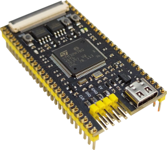
STM32H7B0 · 280MHz
128KB flash · ~1.4MB SRAM
External ST-Link · SWD
Part 2
접을 수 있는 영어 원문 전체
영어 원문 전체 펼치기
BB1D37C96C49BD45F8E205683016A1040FE97AAA05738CED162335768F775E87
.. _fk7b0m1_vbt6:

FANKE FK7B0M1-VBT6
##################

Overview
********

The FK7B0M1-VBT6 core board by FANKE Technology Co., Ltd. is an advanced microcontroller
platform based on the STMicroelectronics Arm® Cortex®-M7 core STM32H7B0VBT6 microcontroller.
This board is an ideal solution for developers looking to create high-performance
applications, especially in the field of Human-Machine Interface (HMI), leveraging its
robust capabilities and support for sophisticated display and touch technologies.

The FK7B0M1-VBT6 is designed as a reference design for user application development before
transitioning to the final product, significantly simplifying the development process.
Its wide range of hardware features, including advanced display and touch capabilities,
make it exceptionally suitable for HMI applications, allowing for comprehensive evaluation
and testing of peripherals and functionalities.

.. figure:: ../../../../../../../boards/fanke/fk7b0m1_vbt6/doc/img/fk7b0m1_vbt6.webp
     :width: 600px
     :align: center
     :alt: FK7B0M1-VBT6

     FK7B0M1-VBT6 (Credit: FANKE Technology Co., Ltd)

Hardware
********

FK7B0M1-VBT6 provides the following hardware components:

- STM32H7B6VB in LQFP100 package
- ARM 32-bit Cortex-M7 CPU with FPU
- 280 MHz max CPU frequency
- VDD from 1.62 V to 3.6 V
- 128 KB Flash
- ~1.4 MB SRAM max (1.18 Mbytes user SRAM + 64 Kbytes ITCM RAM + 128 Kbytes DTCM RAM + 4 Kbytes SRAM in Backup domain)
- Main clock: External 25MHz crystal oscillator.
- RTC: 32.768kHz crystal oscillator.
- 32-bit timers(2)
- 16-bit timers(12)
- 1 reset button, 1 user button, and 1 BOOT button
- 1 user LED
- External 64-Mbit QSPI (W25Q64) NOR Flash memory.
- External 64-Mbit SPI (W25Q64) NOR Flash memory.
- USB OTG Full Speed and High Speed(1)
- 1 micro SD card
- 1 RGB LCD interface
- SWD and serial port accessibility through a pin header
- Bring out 39 IO ports

More information about STM32H7B0VB can be found here:

- `STM32H7B0VB on www.st.com`_

Supported Features
==================

The Zephyr fk7b0m1_vbt6 board configuration supports the following hardware
features:

+-------------+------------+-------------------------------------+
| Interface   | Controller | Driver/Component                    |
+=============+============+=====================================+
| NVIC        | on-chip    | nested vector interrupt controller  |
+-------------+------------+-------------------------------------+
| FLASH       | on-chip    | flash memory                        |
+-------------+------------+-------------------------------------+
| UART        | on-chip    | serial port                         |
+-------------+------------+-------------------------------------+
| PINMUX      | on-chip    | pinmux                              |
+-------------+------------+-------------------------------------+
| GPIO        | on-chip    | gpio                                |
+-------------+------------+-------------------------------------+
| RNG         | on-chip    | True Random number generator        |
+-------------+------------+-------------------------------------+
| Backup SRAM | on-chip    | Backup SRAM                         |
+-------------+------------+-------------------------------------+
| SPI         | on-chip    | spi bus                             |
+-------------+------------+-------------------------------------+
| OCTOSPI     | on-chip    | octospi                             |
+-------------+------------+-------------------------------------+

Other hardware features are not yet supported on this Zephyr port.

The default configuration per core can be found in
:zephyr_file:`boards/fanke/fk7b0m1_vbt6/fk7b0m1_vbt6_defconfig`

Pin Mapping
===========

FK7B0M1-VBT6 board has 5 GPIO controllers. These controllers are responsible for pin muxing,
input/output, pull-up, etc.

.. figure:: ../../../../../../../boards/fanke/fk7b0m1_vbt6/doc/img/fk7b0m1_vbt6_pins.webp
     :width: 600px
     :align: center
     :alt: FK7B0M1-VBT6

     FK7B0M1-VBT6 (Credit: FANKE Technology Co., Ltd)

Default Zephyr Peripheral Mapping:
----------------------------------

The FK7B0M1-VBT6 board is configured as follows

- UART_1 TX/RX : PA9/PA10 (available on the header pins)
- User LED (blue) : PC1
- User PB : PC13
- SPI1 NCS/CLK/MISO/MOSI : PA15/PB3/PB4/PB5 (NOR Flash)
- QuadSPI NCS/CLK/IO0/IO1/IO2/IO3 : PB6/PB2/PD11/PD12/PE2/PD13 (NOR Flash)
- USB DM/DP : PA11/PA12

System Clock
============

The FK7B0M1-VBT6 System Clock could be driven by an internal or external oscillator,
as well as by the main PLL clock. By default the system clock is driven by the PLL clock at 280MHz,
driven by an 25MHz external crystal oscillator.

Serial Port
===========

The Zephyr console output is assigned to UART1. The default communication settings are 115200 8N1.

Programming and Debugging
*************************

Applications for the ``fk7b0m1_vbt6`` board configuration can be built and flashed in the usual
way (see :ref:`build_an_application` and :ref:`application_run` for more details).

Flashing
========

The FK7B0M1-VBT6 board does not include an on-board debugger. As a result, it requires
an external debugger, such as ST-Link, for programming and debugging purposes.

The board provides header pins for the Serial Wire Debug (SWD) interface.

Flashing an application to FK7B0M1-VBT6
---------------------------------------

To begin, connect the ST-Link Debug Programmer to the FK7B0M1-VBT6 board using the SWD
interface. Next, connect the ST-Link to your host computer via a USB port.
Once this setup is complete, you can proceed to build and flash your application to the board

Here is an example for the :ref:`hello_world` application.

.. zephyr-app-commands::
   :zephyr-app: samples/hello_world
   :board: fk7b0m1_vbt6
   :goals: build flash

Run a serial host program to connect with your board:

.. code-block:: console

   $ minicom -D /dev/ttyACM0 -b 115200

Then, press the RESET button, you should see the following message:

.. code-block:: console

   Hello World! fk7b0m1_vbt6

Debugging
=========

This current Zephyr port does not support debugging.

References
**********

.. target-notes::
.. _STM32H7B0VB on www.st.com: https://www.st.com/en/microcontrollers/stm32h7b0vb.html
Part 3
한국어 전문 번역
개요
FANKE Technology Co., Ltd.의 FK7B0M1-VBT6 core board는 STMicroelectronics Arm Cortex-M7 core STM32H7B0VBT6 microcontroller 기반의 advanced microcontroller platform입니다. 강력한 성능과 정교한 display·touch technology 지원을 활용해 특히 Human-Machine Interface(HMI) 분야의 high-performance application을 개발하려는 개발자에게 적합합니다.
FK7B0M1-VBT6는 final product로 전환하기 전에 user application을 개발하는 reference design으로 설계되어 개발 과정을 크게 단순화합니다. Advanced display와 touch 기능을 포함한 폭넓은 hardware는 peripheral과 기능을 포괄적으로 평가·시험할 수 있어 HMI application에 특히 적합합니다.
Hardware
FK7B0M1-VBT6는 다음 hardware component를 제공합니다.
- LQFP100 package의 STM32H7B6VB
- FPU를 갖춘 ARM 32-bit Cortex-M7 CPU
- 최대 CPU frequency 280MHz
- VDD 1.62V~3.6V
- 128KB Flash
- 최대 약 1.4MB SRAM(1.18MB user SRAM + 64KB ITCM RAM + 128KB DTCM RAM + Backup domain의 4KB SRAM)
- Main clock: external 25MHz crystal oscillator
- RTC: 32.768kHz crystal oscillator
- 32-bit timer 2개
- 16-bit timer 12개
- Reset button 1개, user button 1개, BOOT button 1개
- User LED 1개
- External 64-Mbit QSPI(W25Q64) NOR flash
- External 64-Mbit SPI(W25Q64) NOR flash
- USB OTG Full Speed와 High Speed 1개
- micro SD card 1개
- RGB LCD interface 1개
- Pin header를 통한 SWD와 serial port 접근
- 39개 IO port 인출
STM32H7B0VB 정보는 STM32H7B0VB on www.st.com에서 확인할 수 있습니다.
지원 기능
Zephyr fk7b0m1_vbt6 board configuration은 다음 hardware 기능을 지원합니다.
| Interface | Controller | Driver/Component |
|---|---|---|
| NVIC | on-chip | nested vector interrupt controller |
| FLASH | on-chip | flash memory |
| UART | on-chip | serial port |
| PINMUX | on-chip | pinmux |
| GPIO | on-chip | gpio |
| RNG | on-chip | True Random number generator |
| Backup SRAM | on-chip | Backup SRAM |
| SPI | on-chip | spi bus |
| OCTOSPI | on-chip | octospi |
그 밖의 hardware 기능은 아직 이 Zephyr port에서 지원하지 않습니다.
Core별 default configuration은 boards/fanke/fk7b0m1_vbt6/fk7b0m1_vbt6_defconfig에 있습니다.
Pin Mapping
FK7B0M1-VBT6 board에는 GPIO controller가 5개 있으며 pin muxing, input/output, pull-up 등을 담당합니다.
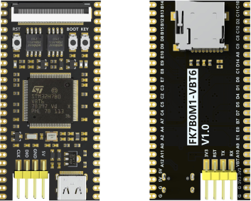
Default Zephyr peripheral mapping
FK7B0M1-VBT6 board는 다음과 같이 구성됩니다.
- UART_1 TX/RX: PA9/PA10(header pin에서 사용 가능)
- User LED(blue): PC1
- User PB: PC13
- SPI1 NCS/CLK/MISO/MOSI: PA15/PB3/PB4/PB5(NOR flash)
- QuadSPI NCS/CLK/IO0/IO1/IO2/IO3: PB6/PB2/PD11/PD12/PE2/PD13(NOR flash)
- USB DM/DP: PA11/PA12
System Clock
FK7B0M1-VBT6 system clock은 internal·external oscillator 또는 main PLL clock으로 구동할 수 있습니다. Default system clock은 25MHz external crystal oscillator가 구동하는 280MHz PLL clock입니다.
Serial Port
Zephyr console output은 UART1에 할당됩니다. Default communication setting은 115200 8N1입니다.
Programming과 Debugging
fk7b0m1_vbt6 board configuration용 application은 일반적인 방법으로 build하고 flash할 수 있습니다.
Flashing
FK7B0M1-VBT6 board에는 onboard debugger가 없어 programming과 debugging에 ST-Link 같은 external debugger가 필요합니다. Board는 Serial Wire Debug(SWD) interface용 header pin을 제공합니다.
FK7B0M1-VBT6에 application flashing
먼저 SWD interface로 ST-Link Debug Programmer를 FK7B0M1-VBT6 board에 연결합니다. 그다음 ST-Link를 USB port로 host computer에 연결하고 application을 build·flash합니다.
hello_world application 예입니다.
west build -b fk7b0m1_vbt6 samples/hello_world
west flash
Serial host program을 실행해 board에 연결합니다.
$ minicom -D /dev/ttyACM0 -b 115200RESET button을 누르면 다음 message가 표시되어야 합니다.
Hello World! fk7b0m1_vbt6Debugging
현재 Zephyr port는 debugging을 지원하지 않습니다.
참고 자료
Source
출처
영어 원문에는 문단, 문서 지시문, 표, 코드, 코드 심벌, 경로를 그대로 보존했습니다.