Part 1
요약·해설
MAX32655EVKIT는 MAX32655 wireless SoC 평가 platform입니다. 100 MHz Cortex-M4F, Bluetooth 5.2 LE와 SIMO power management를 중심으로 color TFT, stereo codec, digital microphone과 QSPI flash를 연결합니다.
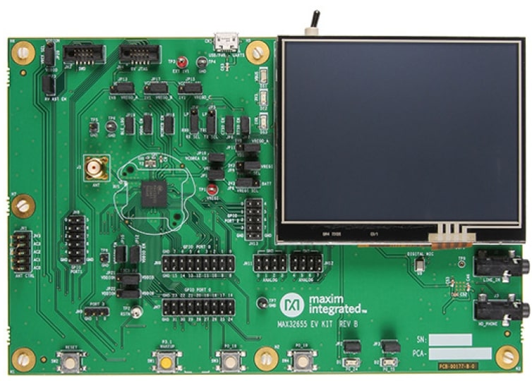
MAX32655 Cortex-M4F, 100 MHz oscillator
Bluetooth 5.2 LE + RISC-V radio coprocessor
TFT, stereo codec, microphone, QSPI flash 128 Mbit
Part 2
접을 수 있는 영어 원문 전체
영어 원문 전체 펼치기
3EB06B181DEA2F5A161186D78CF77673594B2CA189FFCC4F649904660AF48EF5
.. _max32655_evkit:
MAX32655EVKIT
#############
Overview
********
The MAX32655 evaluation kit (EV kit) provides a platform for evaluation capabilities
of the MAX32655 microcontroller, which is an advanced system-on-chip (SoC).
It features an Arm® Cortex®-M4F CPU for efficient computation of complex functions and
algorithms, integrated power management (SIMO), and the newest generation
Bluetooth® 5.0 Low Energy (Bluetooth LE), long-range radio for wearable and hearable device applications.
The Zephyr port is running on the MAX32655 MCU.
.. image:: ../../../../../../../boards/adi/max32655evkit/doc/img/max32655evkit_img1.jpg
:align: center
:alt: MAX32655 EVKIT Front
.. image:: ../../../../../../../boards/adi/max32655evkit/doc/img/max32655evkit_img2.jpg
:align: center
:alt: MAX32655 Back
Hardware
********
- MAX32655 MCU:
- Ultra-Low-Power Wireless Microcontroller
- Internal 100MHz Oscillator
- Flexible Low-Power Modes with 7.3728MHz System Clock Option
- 512KB Flash and 128KB SRAM (Optional ECC on One 32KB SRAM Bank)
- 16KB Instruction Cache
- Bluetooth 5.2 LE Radio
- Dedicated, Ultra-Low-Power, 32-Bit RISC-V Coprocessor to Offload Timing-Critical Bluetooth Processing
- Fully Open-Source Bluetooth 5.2 Stack Available
- Supports AoA, AoD, LE Audio, and Mesh
- High-Throughput (2Mbps) Mode
- Long-Range (125kbps and 500kbps) Modes
- Rx Sensitivity: -97.5dBm; Tx Power: +4.5dBm
- Single-Ended Antenna Connection (50Ω)
- Power Management Maximizes Battery Life
- 2.0V to 3.6V Supply Voltage Range
- Integrated SIMO Power Regulator
- Dynamic Voltage Scaling (DVS)
- 23.8μA/MHz Active Current at 3.0V
- 4.4μA at 3.0V Retention Current for 32KB
- Selectable SRAM Retention + RTC in Low-Power Modes
- Multiple Peripherals for System Control
- Up to Two High-Speed SPI Master/Slave
- Up to Three High-Speed I2C Master/Slave (3.4Mbps)
- Up to Four UART, One I2S Master/Slave
- Up to 8-Input, 10-Bit Sigma-Delta ADC 7.8ksps
- Up to Four Micro-Power Comparators
- Timers: Up to Two Four 32-Bit, Two LP, TwoWatchdog Timers
- 1-Wire® Master
- Up to Four Pulse Train (PWM) Engines
- RTC with Wake-Up Timer
- Up to 52 GPIOs
- Security and Integrity
- Available Secure Boot
- TRNG Seed Generator
- AES 128/192/256 Hardware Acceleration Engine
- External devices connected to the MAX32655 EVKIT:
- Color TFT Display
- Audio Stereo Codec Interface
- Digital Microphone
- A 128Mb QSPI flash
Supported Features
==================
Below are the interfaces supported by Zephyr on MAX32655EVKIT.
+-----------+------------+-------------------------------------+
| Interface | Controller | Driver/Component |
+===========+============+=====================================+
| NVIC | on-chip | nested vector interrupt controller |
+-----------+------------+-------------------------------------+
| SYSTICK | on-chip | systick |
+-----------+------------+-------------------------------------+
| CLOCK | on-chip | clock and reset control |
+-----------+------------+-------------------------------------+
| GPIO | on-chip | gpio |
+-----------+------------+-------------------------------------+
| UART | on-chip | serial |
+-----------+------------+-------------------------------------+
Connections and IOs
===================
+-----------+---------------+-----------------------------------------------------------------------+
| Name | Signal | Usage |
+===========+===============+=======================================================================+
| JP1 | VREGI | Connect/Disconnect VREGIO power |
+-----------+---------------+-----------------------------------------------------------------------+
| JP2 | P0_24 | Enable/Disable LED1 |
+-----------+---------------+-----------------------------------------------------------------------+
| JP3 | P0_25 | Enable/Disable LED2 |
+-----------+---------------+-----------------------------------------------------------------------+
| JP4 | P2_6/ P2_7 | Connect/Disconnect the USB to serial UART to GPIO P2_6 (LPUART_RX) |
+-----------+---------------+-----------------------------------------------------------------------+
| JP5 | P2_7/ P0_1 | Connect/Disconnect the USB to serial UART to GPIO P2_7 (LPUART_TX) |
+-----------+---------------+-----------------------------------------------------------------------+
| JP6 | P0_2 | Connect/Disconnect the USB to serial UART to GPIO P0_2 (UART0_CTS) |
+-----------+---------------+-----------------------------------------------------------------------+
| JP7 | P0_3 | Connect/Disconnect he USB to serial UART to GPIO P0_3 (UART0_RTS) |
+-----------+---------------+-----------------------------------------------------------------------+
| JP8 | VREGI | Select VDDIO_EN power source (3V3 or coin cell) |
+-----------+---------------+-----------------------------------------------------------------------+
| JP9 | VDDIOH_EN | Select VDDIOH_EN power source 3V3/VREGI |
+-----------+---------------+-----------------------------------------------------------------------+
| JP10 | VDDIOH | Connect/Disconnect VDDIOH power |
+-----------+---------------+-----------------------------------------------------------------------+
| JP11 | VDDIO_EN | Select VDDIO_EN power source 1V8/VREGO_A |
+-----------+---------------+-----------------------------------------------------------------------+
| JP12 | VDDIO | Connect/Disconnect VDDIO power |
+-----------+---------------+-----------------------------------------------------------------------+
| JP13 | VDDA_EN | Select VDDA_EN power source 1V8/VREGO_A |
+-----------+---------------+-----------------------------------------------------------------------+
| JP14 | VDDA | Connect/Disconnect VDDA power |
+-----------+---------------+-----------------------------------------------------------------------+
| JP15 | VCOREA_EN | Select VCOREA_EN power source 1V1/VREGO_C |
+-----------+---------------+-----------------------------------------------------------------------+
| JP16 | VCOREA | Connect/Disconnect VCOREA power |
+-----------+---------------+-----------------------------------------------------------------------+
| JP17 | VCOREB_EN | Select VCOREB_EN power source 1V1/VREGO_B |
+-----------+---------------+-----------------------------------------------------------------------+
| JP18 | VCOREB | Connect/Disconnect VCOREB power |
+-----------+---------------+-----------------------------------------------------------------------+
| JP19 | BLE_LDO | Connect/Disconnect BLE_LDO power |
+-----------+---------------+-----------------------------------------------------------------------+
| JP20 | VREF | Select VREF power source VDDIO/VDDIOH |
+-----------+---------------+-----------------------------------------------------------------------+
| JP21 | I2C0_PU | Select I2C0_PU power source VDDIO/VDDIOH |
+-----------+---------------+-----------------------------------------------------------------------+
| JP22 | I2C1_PU | Select I2C1_PU power source VDDIO/VDDIOH |
+-----------+---------------+-----------------------------------------------------------------------+
| JP23 | BOARD RESET | Connect/Disconnect RV JTAG NRESET from the BOARD RESET circuitry |
+-----------+---------------+-----------------------------------------------------------------------+
Programming and Debugging
*************************
Flashing
========
The MAX32655 MCU can be flashed by connecting an external debug probe to the
SWD port. SWD debug can be accessed through the Cortex 10-pin connector, JH3.
Logic levels are fixed to VDDIO (1.8V).
Once the debug probe is connected to your host computer, then you can simply run the
``west flash`` command to write a firmware image into flash.
.. note::
This board uses OpenOCD as the default debug interface. You can also use
a Segger J-Link with Segger's native tooling by overriding the runner,
appending ``--runner jlink`` to your ``west`` command(s). The J-Link should
be connected to the standard 2*5 pin debug connector (JW3) using an
appropriate adapter board and cable.
Debugging
=========
Please refer to the `Flashing`_ section and run the ``west debug`` command
instead of ``west flash``.
References
**********
- `MAX32655EVKIT web page`_
.. _MAX32655EVKIT web page:
https://www.analog.com/en/design-center/evaluation-hardware-and-software/evaluation-boards-kits/max32655evkit.html#eb-overview
Part 3
한국어 전문 번역
개요
MAX32655 evaluation kit는 advanced SoC인 MAX32655 microcontroller의 기능을 평가하는 platform입니다. 복잡한 function과 algorithm을 효율적으로 처리하는 Arm Cortex-M4F CPU, integrated SIMO power management, wearable·hearable application용 최신 Bluetooth 5.0 Low Energy long-range radio를 제공합니다.
Zephyr port는 MAX32655 MCU에서 실행됩니다.
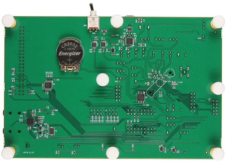
하드웨어
MAX32655 MCU
- Ultra-low-power wireless microcontroller: internal 100 MHz oscillator, 7.3728 MHz system clock 선택이 가능한 low-power mode, flash 512 KB, SRAM 128 KB(32 KB bank 하나에 optional ECC), instruction cache 16 KB.
- Bluetooth 5.2 LE radio: timing-critical Bluetooth 처리를 offload하는 ultra-low-power 32-bit RISC-V coprocessor, open-source Bluetooth 5.2 stack, AoA·AoD·LE Audio·Mesh, 2 Mbit/s high-throughput, 125/500 kbit/s long-range, RX sensitivity -97.5 dBm, TX power +4.5 dBm, 50 Ω single-ended antenna.
- Power management: 2.0~3.6 V supply, integrated SIMO regulator, DVS, 3.0 V에서 active current 23.8 μA/MHz, 32 KB retention current 4.4 μA, low-power mode의 선택적 SRAM retention과 RTC.
- Peripheral: high-speed SPI master/slave 최대 2개, 3.4 Mbit/s I2C master/slave 최대 3개, UART 최대 4개와 I2S master/slave 1개, input 8개의 10-bit sigma-delta ADC 7.8 ksps, micro-power comparator 최대 4개, 32-bit timer·low-power timer·watchdog timer, 1-Wire master, pulse-train PWM engine 최대 4개, wake-up timer를 갖춘 RTC, GPIO 최대 52개.
- Security: secure boot option, TRNG seed generator, AES-128/192/256 hardware acceleration.
MAX32655 EVKIT 외부 device
- color TFT display
- audio stereo codec interface
- digital microphone
- QSPI flash 128 Mbit
지원 기능
Zephyr는 MAX32655EVKIT에서 다음 interface를 지원합니다.
| Interface | Controller | Driver/Component |
|---|---|---|
| NVIC | on-chip | nested vector interrupt controller |
| SYSTICK | on-chip | systick |
| CLOCK | on-chip | clock and reset control |
| GPIO | on-chip | gpio |
| UART | on-chip | serial |
연결과 I/O
| Name | Signal | Usage |
|---|---|---|
| JP1 | VREGI | VREGIO power 연결/해제 |
| JP2 | P0_24 | LED1 enable/disable |
| JP3 | P0_25 | LED2 enable/disable |
| JP4 | P2_6/P2_7 | USB-to-serial UART를 GPIO P2_6(LPUART_RX)에 연결/해제 |
| JP5 | P2_7/P0_1 | USB-to-serial UART를 GPIO P2_7(LPUART_TX)에 연결/해제 |
| JP6 | P0_2 | USB-to-serial UART를 P0_2(UART0_CTS)에 연결/해제 |
| JP7 | P0_3 | USB-to-serial UART를 P0_3(UART0_RTS)에 연결/해제 |
| JP8 | VREGI | VDDIO_EN source 3V3 또는 coin cell 선택 |
| JP9 | VDDIOH_EN | VDDIOH_EN source 3V3/VREGI 선택 |
| JP10 | VDDIOH | VDDIOH power 연결/해제 |
| JP11 | VDDIO_EN | VDDIO_EN source 1V8/VREGO_A 선택 |
| JP12 | VDDIO | VDDIO power 연결/해제 |
| JP13 | VDDA_EN | VDDA_EN source 1V8/VREGO_A 선택 |
| JP14 | VDDA | VDDA power 연결/해제 |
| JP15 | VCOREA_EN | VCOREA_EN source 1V1/VREGO_C 선택 |
| JP16 | VCOREA | VCOREA power 연결/해제 |
| JP17 | VCOREB_EN | VCOREB_EN source 1V1/VREGO_B 선택 |
| JP18 | VCOREB | VCOREB power 연결/해제 |
| JP19 | BLE_LDO | BLE_LDO power 연결/해제 |
| JP20 | VREF | VREF source VDDIO/VDDIOH 선택 |
| JP21 | I2C0_PU | I2C0 pull-up source VDDIO/VDDIOH 선택 |
| JP22 | I2C1_PU | I2C1 pull-up source VDDIO/VDDIOH 선택 |
| JP23 | BOARD RESET | RV JTAG NRESET을 BOARD RESET circuit에 연결/해제 |
프로그래밍과 디버깅
MAX32655 MCU는 JH3 Cortex 10-pin connector의 SWD port에 external debug probe를 연결해 flash할 수 있습니다. logic level은 VDDIO 1.8 V로 고정됩니다. probe를 host에 연결한 뒤 west flash를 실행합니다.
Debugging
같은 연결에서 west flash 대신 west debug를 실행합니다.
참고 자료
Source
출처
영어 원문에는 문단, 문서 지시문, 표, 코드, 코드 심벌, 경로를 그대로 보존했습니다.